Modifying and Overclocking GeForce3
Modifying and Overclocking GeForce3
Using the experience accumulated during the development and support of products based on GeForce2, Nvidia designed and released the GeForce3 chip, with several modifications. The standard GeForce3 chip supports core and memory frequencies of 200 MHz and 460 MHz, respectively. GeForce3 Ti500 supports frequencies of 240 MHz and 500 MHz, and GeForce3 Ti200 supports frequencies of 175 MHz and 400 MHz.
Modifying VisionTek GeForce3
The VisionTek GeForce3 video adapter is manufactured according to the Nvidia reference design (Fig. 14.1).
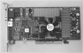
Figure 14.1: VisionTek GeForce3 adapter
The VisionTek adapter has an AGP 2x/4x interface and is equipped with 64 MB of DDR SDRAM, represented by eight chips installed on the front side of the printed circuit board (PCB).
The adapter is equipped with memory chips from Elite Semiconductor Memory Technology (ESMT, sometimes referred to as EliteMT), with an access time of 3.8 nanoseconds. This corresponds approximately to a clock frequency of 263 MHz (and a data-transmission frequency of approximately 526 MHz). According to the specification, the memory operates at a frequency of 230 (460) MHz.
The adapter is equipped with SC1175CSW stabilizers from Semtech, which are duplicated pulse-duration controllers. These chips are intended mainly for memory power-supply stabilizers installed on video adapters and peripheral devices. Two independent controllers of these chips can operate in two modes: independently or with current sharing.
To obtain a stabilized core supply voltage of the GeForce3 adapter, the current sharing mode is used. In this mode, the output voltage of the first controller is specified by the resistor ratio (R1:R12 on a typical connection layout). The second controller uses the output voltage from the first one as a reference. Its output is connected to the output of the first controller, which means that two built-in stabilizers operate in parallel. Hence, the name of this mode is current sharing.
The typical method of connecting the stabilizers in this mode is shown in Fig. 14.2. The following formulas are applicable:
| (Formula 14.1) |
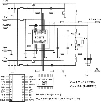
Figure 14.2: Design of stabilizer connection
| (Formula 14.2) |
| (Formula 14.3) |
| (Formula 14.4) |
On VisionTek GeForce3, the resistance of R12 and R1 (R832 and R810 on the PCB) is 130 ohms and 770 ohms, respectively. Output voltage, calculated using Formula 14.1, is 1.45 V.
In the course of modification, the R1 resistor was shunted by a 510-ohm resistor, soldered to the contacts labeled 18 and 20 on the SC1175CSW chip (Fig. 14.3). As a result, the output voltage changed to 1.78 V.
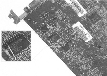
Figure 14.3: SC1175CSW chip
Because another SC1175CSW chip was installed on the board to supply power to the video memory, it became possible to increase the video-memory power-supply voltage.
The chip channels operate independently, and the output voltage of each is set individually by the divider. A typical method of connecting a chip in the mode with two independent channels is shown in Fig. 14.4.
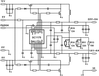
Figure 14.4: Method of connecting a chip in the mode with two independent channels
According to the specification, DDR SDRAM memory chips used with GeForce3 are supplied with two voltages: 3.3 V and 2.5 V. One channel of the SC1175CSW chip ensures power supply to the internal circuitry of the video memory chips; another supplies voltage for input/output buffers.
Output voltages for the channels are set by the R15:R14 resistor ratio for the 3.3 V channel, and R13:R11 for the 2.5 V channel.
Resistors installed on the board (R822:R824 for 3.3 V, and R825:R829 for 2.5 V) have resistance values of 170 ohms, 100 ohms, 110 ohms, and 100 ohms, respectively. Coupled, they ensure output voltages of 3.37 V and 2.63 V, which means that the supply voltages for the video memory are already slightly higher than the nominal values. To increase these voltages further, R14 and R11 were shunted. To achieve this, 820-ohm resistors were soldered to the chip output contacts labeled 3, 18, and 20, as shown in Figs. 14.5 and 14.6.
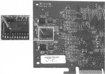
Figure 14.5: Additional resistance (view of contact 3)
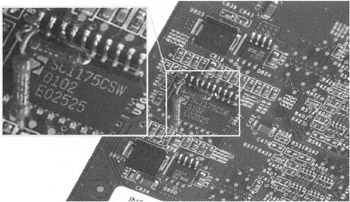
Figure 14.6: Additional resistance (view of contacts 18 and 20)
As a result, the "new" resistance values for R14 and R11 were 89 ohms each, and the output voltages of the chip channels, calculated using the same formula, were 3.64 V and 2.8 V.
Increasing the core voltage and the video-memory supply voltage drastically increases the chip workloads and results in intense heat emission. Therefore, it is necessary to consider efficient cooling. To improve the temperature mode, specially designed heatsinks from Thermaltake were installed on the memory chips. To cool the video core, it was equipped with a heatsink taken from a standard ND3 processor cooler and an efficient fan from a Thermaltake Volcano cooler (Fig. 14.7).
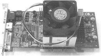
Figure 14.7: Cooling facilities
This cooling system seemed to be insufficient; therefore, a variant with a Peltier element also was tried. Because of the high efficiency of such a cooling system, the GeForce3 chip retained stability at frequencies of 280 MHz to 290 MHz. However, after a drop of the condensation trickled into the AGP, only luck kept the motherboard and video adapter from failing. Therefore, the Peltier element was abandoned. Without it, the video chip overheated at a frequency of 270 MHz, and the system hung up.
During experiments, it was discovered that the surface of the GeForce3 chip is curved inward. This made it difficult to ensure normal heat evacuation from the small, round metal surface bent inward. The solution to this problem requires leveling and polishing the chip surface (Fig. 14.8).
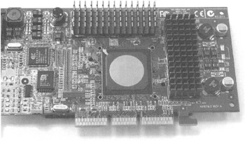
Figure 14.8: Leveled and polished video chip
The surface of the GeForce3 chip and the base of the heatsink were polished, it became possible to achieve stable operation of the video adapter at high frequencies. As a result of this modification, the VisionTek adapter operated reliably at a 270 MHz core frequency and a 600 MHz (300 MHz DDR) video memory frequency. All video adapters based on Nvidia GeForce3 are equipped with DDR SDRAM chips with an access time of 3.8 nanoseconds; therefore, this value of the video memory frequency is a great result.
Modifying Asus V8200
The Asus V8200 video adapter is implemented on the PCB with a design different from the reference one. Nevertheless, the core and video-memory power-supply stabilizers are the same ones used for the previous adapter. The only difference lies in the positioning of their elements (Fig. 14.9).
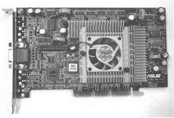
Figure 14.9: Asus V8200 adapter
Resistors specifying the core voltage (on the board, they are labeled R134 and R138) are on the underside of the board. Their resistance is 140 ohms and 780 ohms, respectively. The power supply voltage of the Nvidia GeForce3 chip on this adapter is 1.48 V. After installing an additional 820-ohm resistor connected in parallel to R1 (R138 on board), it became possible to obtain a "new" R1 value of 400 ohms (Fig. 14.10).
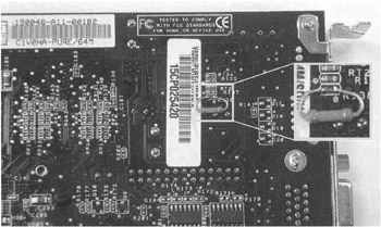
Figure 14.10: Resistor correcting the video core voltage
The voltage at the stabilizer output is 1.68 V. Because of the highly efficient cooling system, the core temperature on Asus V8200 didn't rise as significantly as that of the VisionTek adapter. Therefore, additional steps for cooling the core were not required.
The video-memory supply voltage was raised as it was for VisionTek GeForce3 (Figs. 14.11 and 14.12). Two 820-ohm resistors were used for this purpose.
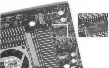
Figure 14.11: Raising the memory supply voltage
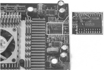
Figure 14.12: Raising the memory supply voltage (continued)
After this modification, the video adapter from Asus operated at a 260 MHz core frequency and a 580 MHz (290 MHz DDR) video memory frequency.
Overclocking and Testing
The following hardware configuration was used to test the video adapters:
-
Processor — AMD Athlon 1,200 MHz (133 MHz FSB frequency)
-
Motherboard — Abit KT7A (VIA KT133A)
-
RAM — 256 MB, NCP PC133
-
Hard disk — Fujitsu MPE3084AE, 8.4 GB
The following software was used:
-
Driver — DirectX8.la
-
Operating system — Windows 98 SE, build 4.10.2222 A
-
Test — Quake III Arena v1.27g
Video adapters were tested with the Detonator 12.41 driver. To set the core and video memory clock frequencies, the RivaTuner utility was used.
To improve the temperature conditions of the hardware components, the test system was assembled without a case. Because of this, there were no problems with removing the hot air typical of systems assembled in closed cases. A standard 80 mm fan was placed in front of the video adapter, at a distance of 5 cm to 10 cm. This fan ensured forced air cooling of the heatsinks installed on the video memory chips. The temperature in the test room was between 20°C (68°F) and 23°C (73°F).
The tests were conducted using the VisionTek GeForce3 video adapter, which showed more stable operation than Asus V8200 did at a high frequency.
Using Quake III Arena as a game test, the VisionTek adapter was tested at the following settings: For the modes with a color depth of 16 bits, 16-bit textures were chosen. For 32-bit modes, 32-bit textures were used. The texture quality and geometry details were set at maximum. Trilinear texture filtering was enabled; compression was disabled.
Graphs illustrating performance growth as a percentage of the results achieved at nominal frequencies are provided in Figs. 14.13 and 14.14.
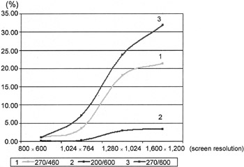
Figure 14.13: Performance evaluation in 16-bit modes (1–3 show the core/memory frequency in megahertz)
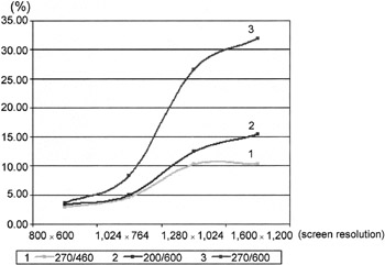
Figure 14.14: Performance evaluation in 32-bit modes (1–3 show the core/memory frequency in megahertz)
At screen resolutions set to 800 × 600 and 1,024 × 768, the performance was limited by the clock frequency of the processor and by overall system performance. As a result, performance growth under conditions of extreme overclocking did not exceed 10%. With higher screen resolutions, it increased more than 30%.
In 16-bit modes, core overclocking ensured more dramatic performance growth than overclocking of video memory.
In 32-bit modes, the performance gain obtained by overclocking the video memory and the core was approximately the same. With an increased screen resolution, video memory overclocking became more efficient, but the performance gain obtained by core overclocking stabilized at 10%.
In 16-bit modes, core overclocking, as was expected, produced more impressive results. Changing the video memory frequency from 460 MHz to 600 MHz had a weak effect at the nominal core frequency, but it provided more significant growth when the core frequency was increased.
In 32-bit modes, video memory overclocking was more efficient. Core overclocking also ensured performance growth, especially when the video memory frequency operated at an increased frequency.
Conclusion
For those who are not satisfied with the performance ensured by GeForce3 video adapters and who are not discouraged by the difficulties and risk of failure encountered when implementing overclocked modes, there is another solution — extreme overclocking. By raising the supply voltage not only for the core, but also for the video memory, it becomes possible to increase the operating frequencies to values that are fantastic for GeForce3 — 270/600 MHz. This makes it possible to obtain a video adapter with excellent performance under the most challenging conditions.


