Modifying and Overclocking GeForce4 Ti4400
Modifying and Overclocking GeForce4 Ti4400
VisionTek Xtasy GeForce4 Ti4400 is implemented according to the Nvidia reference design, and is practically undistinguishable from Nvidia products. The only indication of the manufacturer is the small sticker with VisionTek logo on the cooler (Fig. 14.33).
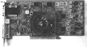
Figure 14.33: VisionTek Xtasy GeForce4 Ti4400 adapter
This video adapter is equipped with the Nvidia GeForce4 Ti4400 graphical chip and has 128 MB of DDR SDRAM from Samsung for video memory, with a clock time of 3.6 nanoseconds.
The maximum frequencies achieved when overclocking Xtasy GeForce4 Ti4400 are 300/660 MHz.
Raising the Video-Core and Video-Memory Supply Voltages
The SC1175CSW chip is responsible for supplying voltage to the graphical core. The methods of increasing the supply voltage were described previously in this chapter.
To increase the supply voltage of the video core, it is possible to decrease the R1 resistor by shunting. (See the typical connection design in Fig. 14.35.) For this purpose, an additional resistor was soldered to the chip outputs labeled 18 and 20 (Fig. 14.34).
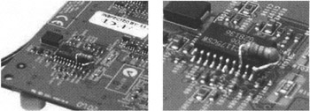
Figure 14.34: Increasing the video-core supply voltage on VisionTek Xtasy GeForce4 Ti4400
The adapter uses 130-ohm and 390-ohm resistors as R1 and R12 (numeration according to the typical method). As a result, the video-core supply voltage is 1.66 V by default. When R1 was shunted with an additional 620-ohm resistor, the video-core supply voltage reached 1.92 V.
The adapter is equipped with video memory chips from Samsung. These chips have a supply voltage for internal circuitry and input/output buffers (Vdd/Vddq) of 2.8 V. This voltage is formed by the SC1102CS chip from Semtech.
This chip operates according to the same principles as the SC1175CSW chip. However, it has only one channel, instead of the two independent channels in SC1175CSW. Another important difference is that the reference voltage in SC1102CS is 1.265 V, rather than 1.25 V in SC1175CSW. Consequently, the output voltage of the stabilizer must be calculated according to the following formula:
| (Formula 14.8) |
In this formula, the resistors are numbered according to the typical connection design (as shown in Fig. 14.35).
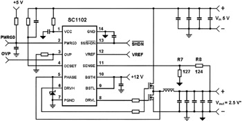
Figure 14.35: Typical connection design for the SC1102CS chip
As previously mentioned, video adapters based on Nvidia GeForce3/Ti200/Ti500 have video memory chips with independent supplies of internal circuitry and input/output buffers (3.3/2.5 V = Vdd/Vddq). In contrast, in video adapters based on Nvidia GeForce4, the Vdd and Vddq circuits of the video memory are connected electrically. The input/output buffers of the GeForce4 chip are supplied with the same voltage as the input/output buffers of the video memory chips. This significantly limits the possibilities of raising the supply voltage: For example, when Vdd/Vddq is raised to 3.0 V, "ripples" appear in text modes. This should not be allowed.
Fortunately, the reference design of the adapter allows an additional stabilizer to be installed that supplies the input/output buffers of the video memory chips when necessary (i.e., when the supply voltages of the internal circuitry and the input/output buffers of the video memory chips are different). Before installing an additional stabilizer, it is necessary to remove the connection between Vdd and Vddq by unsoldering the bridges on the front side of the video adapter (Fig. 14.36). The underside of the adapter is shown in Fig. 14.37.
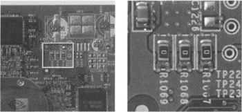
Figure 14.36: VisionTek Xtasy GeForce4 Ti4400 bridges (front side)
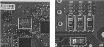
Figure 14.37: VisionTek Xtasy GeForce4 Ti4400 bridges (underside)
Having accomplished this, it is necessary to unsolder the voltage stabilizer that supplies power to the input/output buffers of the video memory chips. (The positions for installing the components are visible in Figs. 14.36 and 14.37.) This task is not difficult, especially for an experienced specialist. However, using a normal diode is simpler. On directly connected silicon diodes, the voltage drop is normally 0.7 V to 0.8 V. Therefore, it is possible to increase the supply voltage of the internal circuitry of the video memory chips (Vdd) while supply power to the input/output buffers from Vdd via the diode.
This approach was chosen in this example. First, the output voltage at the stabilizer was raised to 3.51 V by soldering a 270-ohm resistor to pins 11 and 14 of the SC1102CS chip (Fig. 14.38).
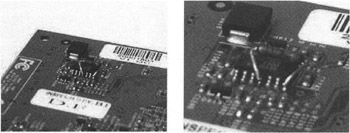
Figure 14.38: Increasing the video-memory supply voltage on VisionTek Xtasy GeForce4 Ti4400
Thus, the supply voltage of the internal circuitry of the video memory chips was increased from 2.82 V to 3.51 V.
Next, the powerful silicon diode was chosen and soldered to the position that was previously occupied by the bridges (Fig. 14.39).
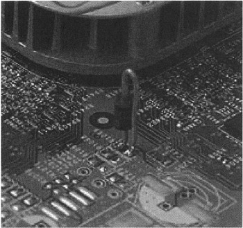
Figure 14.39: Additional diode
After that, the supply voltage of the input/output buffers of the video memory chips and graphical core was 2.77 V. This resulted from the 0.74 V drop on the diode.
After increasing the voltage, it was necessary to consider an efficient cooling system. Overclocking shortens the life of a video adapter. Overclocking combined with an increased supply voltage makes adapter components work overtime. By implementing an efficient cooling system, it is possible to achieve stable operation of the graphical core and video memory at increased frequencies and to prolong the adapter's life as well.
Improving the Cooling System
First, it was necessary to level the surface of the video chip (Fig. 14.40).
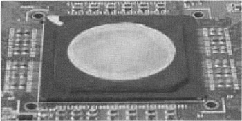
Figure 14.40: Video chip after its surface has been leveled and polished
After that, a powerful cooler was installed on the video chip (Fig. 14.41).
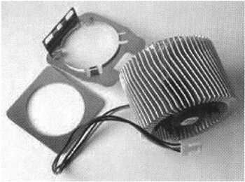
Figure 14.41: Thermaltake Mimi Copper Orb cooler
The fins of the heatsink of the cooler were fastened to the video chip using nylon clips that were passed through the holes in the board.
The final step implies installing heatsinks on the video memory chips. For this purpose, heatsinks supplied in the Thermaltake Memory Cooling Kit were used. Heatsinks were fastened using adhesive thermal stickers from this kit.
After the cooling system was reinforced, the Xtasy GeForce4 Ti4400 adapter looked as shown in Fig. 14.42
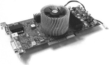
Figure 14.42: VisionTek Xtasy GeForce4 Ti4400 with a modified cooling system
Maximum frequencies at which the modified adapter operated reliably made 340/710 MHz (355 MHz DDR) for video adapter and video memory, respectively. For the moment, this is a record for the products based on Nvidia GeForce4 Ti4400. By achieved frequencies, this modified adapter is far ahead even GeForce4 Ti4600.
Overclocking and Testing
The following hardware configuration was used to test the modified video adapters:
-
Processor — AMD Athlon XP 2000+
-
Motherboard — MSI K7T266 Pro2 v2.0 (VIA KT266A)
-
RAM — 2 × 256 MB, DDR SDRAM, PC 2700, Crucial CL2.5
-
Hard disk — Fujitsu MPF3153AH
The following software was used:
-
Driver — Nvidia Detonator v. 28.32 for Windows XP
-
Operating system — Windows XP
-
Tests — Codecult Codecreatures and 3DMark2001 SE
In the Codecult Codecreatures test, the default settings were used.
The following parameters specified the 3DMark2001 operating mode: 32-bit frame buffer, 32-bit textures, 32(24)-bit Z-buffer, and D3D Pure Hardware T&L.
Codecreatures places a very heavy workload on the video adapter. This is visible even without measuring the number of frames per second.
The large number of polygons in the nature scene (500,000 and more) and stringent requirements of the fill rate manifested — overclocking the video core proved to be more fruitful that overclocking the video memory (Fig. 14.43).
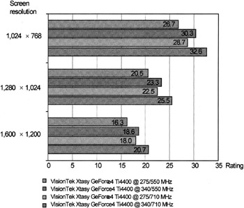
Figure 14.43: Test results obtained using Codecult Codecreatures
In the 3DMark 2001 Nature test (Fig. 14.44), the reverse occurred: Video-memory overclocking was more efficient than video-core overclocking. This can be easily explained: In the Nature test, the number of polygons in each scene is considerably smaller.
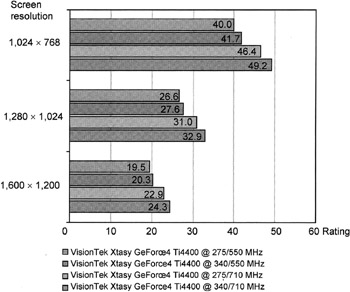
Figure 14.44: Test results obtained using 3DMark2001 (Nature)
Conclusion
The percentage increase of the video core and video memory frequencies obtained by extreme overclocking with Nvidia GeForce4 was not as impressive as with Nvidia GeForce3. However, it is essential to remember that GeForce3 and GeForce4 are manufactured according the same technology — 0.15 micrometer. It's no wonder that video adapters of the GeForce4 generation, which have higher nominal frequencies, have lower overclocking potential. Overclocking potential increases only after migration to more advanced manufacturing technologies.
Although extreme overclocking of GeForce4 Ti4400 is a tedious and troublesome task, the performance increase of 20%–25% is impressive. By implementing this performance reserve, it is possible to enjoy full-screen smoothing, anisotropic filtering, and a high screen resolution.


