Chapter 4: Main Components and the Optimal Choice
Chapter 4: Main Components and the Optimal Choice
The main computer hardware components are the processor, RAM, video adapter, motherboard, and hard disk. The entire system configuration depends on the components chosen. Functional capabilities of the computer and overall system performance in both nominal and overclocked modes depend on the properties of these components and the efficiency of their operation.
Depending on the configuration, the components supplied by different manufacturers might have different parameters and properties. Accounting for specific features allows you to choose the optimal configuration, based on financial limitations and planned tasks.
Processors
The processor is a central element of any computer system. Currently, the most popular and widely used processors are the ones manufactured by Intel (which holds more than 75% of the market) and AMD. Besides these market leaders, another large manufacturer of processors for PCs is Via Technologies.
Intel Pentium III/Celeron (Coppermine)
Intel Pentium III processors with the Coppermine core were based on experience accumulated by developing and running Pentium II, Pentium III, and Celeron (Mendocino).
The first representatives of the Pentium III processor line were released by the end of 1999. Pentium III processors based on the Coppermine core are manufactured using 0.18-micrometer technology. Similar to the earlier Pentium III processors based on the Katmai core, the successors support MMX and SSE. In contrast to their predecessors, they have an integrated L2 cache of 256 KB intended to operate at the core frequency. This makes them similar to the Celeron processors based on the Mendocino core. However, in Coppermine-based processors, L2 cache memory has become larger, the internal bus has been extended from 64 bits to 256 bits, the algorithm of operation has been enriched (256-bit Advanced Transfer Cache), and the core architecture has been improved. These factors allow the processor to achieve higher performance. Performance has improved not only in comparison to the overclocked Celeron (Mendocino) processors, but also in comparison to the Pentium III (Katmai) processors with 512 KB of cache memory, operating at the same frequencies.
In the Pentium III (Coppermine) processor line, some models are intended to operate at the bus frequencies of both 100 MHz and 133 MHz. The latter have the B character in their marking, distinguishing them from processors intended to operate at a 100 MHz bus frequency. Models that have the same frequencies as Pentium III (Katmai) processors are labeled with the E character.
As form factors, SECC2 (Slot 1) and FC-PGA (Flip Chip-Pin Grid Array) (Socket 370) were chosen. Gradually, processors designed using the Socket 370 standard have replaced their predecessors (Figs. 4.1–4.4).
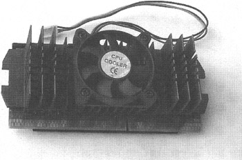
Figure 4.1: Pentium III processor with the SECC2 (Slot 1) form factor, heatsink, and fan
Note that all Pentium III (Coppermine) processors have a fixed multiplier that relates internal and external frequencies; therefore, overclocking can occur only if the processor bus (external) frequency is increased.
Many of the first models of this processor line, intended for a 100 MHz bus frequency, easily allowed the Front Side Bus (FSB) frequency to be increased to 133 MHz or further.
Pentium III (Coppermine) processors have repeated the success of their predecessors. Their overclocking potential confirms that processors of this type have significant technological reserve. This reserve allows both external and internal frequencies to be increased considerably. This increase is accompanied by processor performance growth and, consequently, an increase in overall system performance.
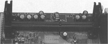
Figure 4.2: Slot 1 processor slot
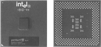
Figure 4.3: Pentium III processor with the FC-PGA (Socket 370) form factor
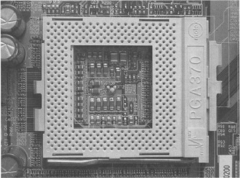
Figure 4.4: Socket 370 processor slot
To provide a more precise evaluation of the temperature mode and appropriate selection of cooling devices, the data on the thermal power dissipated by Pentium III Katmai (512KB L2) and Coppermine (256KB L2) processors are provided in Tables 4.1–4.3.
|
Processor model |
Maximum thermal power (W) |
|---|---|
|
533EB |
14.0 |
|
550E |
14.5 |
|
600E |
15.8 |
|
600EB |
15.8 |
|
650 |
17.0 |
|
667 |
17.5 |
|
700 |
18.3 |
|
733 |
19.1 |
|
750 |
19.5 |
|
800 |
20.8 |
|
800EB |
20.8 |
|
850 |
22.5 |
|
866 |
22.9 |
|
933 |
25.5 |
|
1000B |
33.0 |
|
Processor model |
Maximum thermal power (W) |
|---|---|
|
500E |
13.2 |
|
533EB |
14.0 |
|
550E |
14.5 |
|
600E |
15.8 |
|
600EB |
15.8 |
|
650 |
17.0 |
|
667 |
17.5 |
|
700 |
18.3 |
|
733 |
19.1 |
|
750 |
19.5 |
|
800 |
20.8 |
|
800EB |
20.8 |
|
850 |
22.5 |
|
866 |
22.9 |
|
933 |
24.5 |
|
Processor model |
L2 cache memory (KB) |
Maximum thermal power (W) |
|---|---|---|
|
450 |
512 |
25.3 |
|
500 |
512 |
28.0 |
|
533B |
512 |
29.7 |
|
533EB |
256 |
14.0 |
|
550 |
512 |
30.8 |
|
550E |
256 |
14.5 |
|
600 |
512 |
34.5 |
|
600B |
512 |
34.5 |
|
600E |
256 |
15.8 |
|
600EB |
256 |
15.8 |
Soon after the development and release of the first Pentium III processors based on the Coppermine core, similar low-end processors — Celeron (Coppermine) — were released. These processors appeared as a result of Intel's policy to separate market segments based on the performance and price of products, aimed at optimizing the price:performance ratio.
Celeron processors based on the Coppermine core, in contrast to their more powerful analogues, have less L2 cache memory: 128 KB (256-bit Advanced Transfer Cache). Like the previous core, these processors are intended to operate at a processor-bus frequency of 66 MHz; starting with the Celeron 800MHz processors, they operate at a bus frequency of 100 MHz. In all other aspects, the architecture of these processors resembles that of Pentium III (Coppermine) — including MMX and SSE support, which previously had been exclusive to Pentium III (Katmai) processors. As you may recall, Pentium III (Katmai) processors were oriented toward high-end computers.
Celeron (Coppermine) processors use the FC-PGA (Socket 370) standard.
The first processors of this line, including Celeron 533A (Coppermine), have a 1.5 V core supply voltage, a slightly lower voltage than the similar parameter for Pentium III (Coppermine) processors (1.6 V and 1.65 V). As a rule, this circumstance allows the core supply voltage for Celeron (Coppermine) to be raised to 1.6 V or 1.65 V without serious risks (only if efficient cooling is provided). This has a positive effect on system stability under conditions of extreme overclocking. For later, more powerful Celeron models, the core supply voltage was increased to the levels typical for standard processors based on the Coppermine architecture. This increase of the core supply voltage widens the overclocking capabilities for processors of this type. For example, Celeron 667 (Coppermine) allows overclocking to 1,000 MHz. Generally, Celeron (Coppermine) processors retain stable operation in overclocked modes even at standard core supply voltages, allowing the bus frequency to be exceeded by 30%. Some models allow both internal and external frequencies to be exceeded, providing the potential for 50% performance improvement.
Table 4.4 provides a more precise analysis of the temperature mode of the computer. The data show the thermal power dissipated by the first members of the Celeron processor family, based on the Coppermine core.
|
Processor model |
Maximum thermal power (W) |
|---|---|
|
533A |
11.2 |
|
566 |
11.9 |
|
600 |
12.6 |
|
633 |
16.5 |
|
667 |
17.5 |
|
700 |
18.3 |
Intel Pentium III/Celeron (Tualatin)
Traditional processor architecture based on the Coppermine core and 0.18-micrometer technology reached its limit with the release of models characterized by a 1 GHz to 1.13 GHz clock frequency. For the latest processors based on the Coppermine core, this limit is 1.2 GHz to 1.3 GHz. This evaluation can be proved by analysis and approximation of the results obtained by overclocking various models of processors based on this core.
A greater increase in the CPU core frequency could be achieved only by improving the technological process. This occurred with the transition to the 0.13-micrometer scale. The new core, known as Tualatin, has become the basis for a new processor line.
The design of the Tualatin core, which used Coppermine as a prototype, makes it possible to increase the processor clock rate and solve problems with stable operation at an acceptable level of energy consumption and heat emission. The price of the new processors remains reasonable.
Using the Tualatin core, Intel released Pentium III processors with the following nominal frequencies: 1 GHz, 1.13 GHz, 1.20 GHz, or 1.33 GHz. The basic characteristics of these processors include the amount of L2 cache memory (256 KB) and the FSB frequency (133 MHz).
In addition to Pentium III processors, the traditional low-end line of Celeron processors was released (Fig. 4.5). This line comprises models with a clock frequency of 0.9 GHz, 1 GHz, 1.1 GHz, 1.2 GHz, 1.3 GHz, or 1.4 GHz. The amount of L2 cache memory is 256 KB (as in Pentium III); however, the FSB frequency is only 100 MHz.
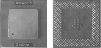
Figure 4.5: Celeron processor with the FC-PGA2 (Socket 370) form factor
The main feature of the new core based on 0.13-micrometer technology is a new approach to the core power supply.
Thinner transistor control gates, the basis of the processor core, made it possible to decrease the levels of the power supply voltage. The intensity of the field that controls the sink-gate current via transistors decreases with the decrease in distance between electrodes. This allowed Intel to lower the levels of the supply voltage to 1.475 V to 1.5 V. For comparison, this parameter in the Coppermine core is 1.6 V to 1.75 V.
However, this is not the sole feature that characterizes the power supply of the processors. When discussing products based on the Tualatin core, it is incorrect to only speak about core voltage.
This processor, in contrast to processors of previous generations, has no constant core voltage level.
The consumption currents of processors have reached a high value. For the latest models of Pentium III (Coppermine), this current reaches 20 amperes. Such a high level is a serious load — not only for processor cores (a surface area of 1 cm2), but also for power supply units. High levels of electric power are dangerous for processor chips because they inevitably are accompanied by significant heat emission. This often leads to local overheating of semiconductors. Besides violation of thermal modes required for proper operation of semiconductors, the chips are exposed to significant dynamic loads, which can destroy internal structures mechanically due to uneven expansion of the chip.
To solve the problem of CPU temperature-mode optimization, Intel developers replaced the constant core voltage level with a variable voltage level. The core voltage now depends on the consumption current, the value of which depends on the processor workload. The higher the current, the lower the processor's core voltage. This voltage decreases from the initial level, stated in the processor specification and set by the Voltage Identification (VID) contacts, to approximately 0.2 V at the maximum workload of the latest models.
As a result, it became necessary to introduce the changes into the Voltage Regulator Module (VRM) specifications. This module, integrated into the motherboard, converts standard voltage delivered by the power supply unit to the level required for correct operation of the processor core. For processors based on the Tualatin core, the VRM module of the motherboard must comply with the 8.5 specification (Fig. 4.6).
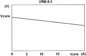
Figure 4.6: Changing the core supply voltage, depending on the consumed current (Icore), in accordance with the 8.5 specification
The power supply of Pentium 4 and Celeron with Socket 478 slots is organized the same way.
The previously mentioned changes also relate to the FSB: The amplitude of transmitted pulses was decreased to 1.25 V. (Previously, this level was 1.5 V.)
Support for processors based on the Tualatin core is implemented in newer motherboards based on special chipset models. In models oriented toward desktop PCs, this is the modified version of the 810E2 chipset and the 815 (Step B) chipset family from Intel. The latter is represented by the following models: 815, 815P, 815G, 815E, 815EP, and 815EG.
Besides this, support for these processor models is implemented by system logic sets from Ali, SiS, and Via Technologies. These chipsets are based on well-known sets and usually have the T character in their marking. The list of such products includes Ali Aladdin Pro 5T from Ali; SiS630ET, SiS630ST, SiS633T, and SiS635T from SiS; and VIA Apollo PLET, VIA Apollo Pro133T, VIA Apollo Pro266T, VIA ProSavage PL133T, VIA ProSavage PN133T, and VIA ProSavageDDR PN266T chipsets designed and manufactured by Via Technologies.
Chipsets from Intel, Ali, SiS, and Via, in combination with VRM 8.5, implement support not only for processors based on the Tualatin core, but also for earlier processors based on the Coppermine core.
Intel Pentium 4/Celeron (Willamette, Northwood)
Intel Pentium 4 processors have principally new architecture (Fig. 4.7). They are based on the Intel NetBurst microarchitecture. The first models were released in 2000. They contained 42 million transistors and were created using a well-checked 0.18-micrometer technology, tested on previous-generation processors. The new core was named Willamette.
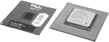
Figure 4.7: Pentium III (Coppermine, Socket 370) and Pentium 4 (Willamette, Socket 423) processors
The usage of hyperpiping technology in the Pentium 4 architecture allowed Intel to significantly increase the operating frequency. The first processors of this line have operating frequencies of 1.3 GHz, 1.4 GHz, 1.5 GHz, and so on.
To ensure nonstop operation of the long pipeline (20 steps) at a high frequency, significant modifications had to be introduced into internal core architecture. For example, the Advanced Dynamic Execution Engine technology improves branch prediction, and the Arithmetic Logic Unit (ALU) operates at the doubled core frequency.
High performance comes with efficient operation of the on-die L1 cache memory (8 KB) and L2 cache memory (256 KB in the Willamette core). As with Pentium III (Coppermine), L2 cache is connected via a 256-bit bus (Advanced Transfer Cache). It operates at the core frequency, ensuring high efficiency of cache operation.
The command set was extended to optimize the operation of internal core units. The additional command set, a further evolution of the MMX and SSE technologies, became known as SSE2 (Streaming SIMD Extensions 2, 144 new instructions).
Such innovations positioned Pentium 4 as a powerful processor oriented toward tasks with minimal branches, such as working with the Internet and processing multimedia information. The share of such tasks is growing steadily.
The high operating frequency required not only a radical redesign of the entire internal processor structure, but also the introduction of appropriate modifications into computer architecture. The processor bus at the 100 MHz frequency transfers data at the frequency of 400 MHz (quad-pumped, or 4X) when passing and processing the address portion at 200 MHz (2X). The next version of this standard implies increasing the bus frequency to 133 MHz, which ensures a data-transfer rate of 533 MHz, as a flow with a throughput of 4.3 GB/sec.
Pentium 4 (Willamette) processors are released in two forms of FC-PGA packaging, with provisions for Socket 423 and Socket 478 slots. The core voltage (Vcore) of processors complying with the Socket 423 standard is 1.7 V and 1.75 V; for processors with Socket 478, it is 1.75 V.
Tables 4.5 and 4.6 outline the main temperature parameters of Pentium 4 and Celeron processors based on the Willamette core. These processors are oriented toward systems with Socket 423 and Socket 478 processor slots, and with data-transfer rate through the system bus equal to 400 MHz. These tables provide clock frequencies, core voltage levels (Vcore), maximum thermal power, and maximum case temperature (Tcase).
|
Processor (GHz)/Vcore (V) |
Maximum thermal power (W) |
Maximum Tcase (°C) |
|---|---|---|
|
1.3/1.7 |
48.9 |
69 |
|
1.4/1.7 |
51.8 |
70 |
|
1.5/1.7 |
54.7 |
72 |
|
1.3/1.75 |
51.6 |
70 |
|
1.4/1.75 |
54.7 |
72 |
|
1.5/1.75 |
57.8 |
73 |
|
1.6/1.75 |
61.0 |
75 |
|
1.7/1.75 |
64.0 |
76 |
|
1.8/1.75 |
66.7 |
78 |
|
1.9/1.75 |
69.2 |
73 |
|
2.0/1.75 |
71.8 |
74 |
|
Processor (GHz) |
Maximum thermal power (W) |
Maximum Tcase (°C) |
|---|---|---|
|
1.4 |
55.3 |
72 |
|
1.5 |
57.9 |
73 |
|
1.6 |
60.8 |
75 |
|
1.7 |
63.5 |
76 |
|
1.8 |
66.1 |
77 |
|
1.9 |
72.8 |
75 |
|
2.0 |
75.3 |
76 |
Using the experience accumulated through developing, manufacturing, and operating Pentium 4 (Willamette), Intel has released a low-end processor line based on the same core. These processors received the traditional name: Intel Celeron. In contrast to the more powerful Pentium 4 processors, this line is characterized by a smaller L2 cache: 128 KB, instead of 256 KB. In other respects, the architecture remained practically unchanged.
Table 4.7 lists the temperature parameters of the first Celeron model based on the Willamette core.
|
Processor (GHz) |
Maximum thermal power (W) |
Maximum Tcase (°C) |
|---|---|---|
|
1.7 |
63.5 |
76 |
The well-tested NetBurst microarchitecture was the basis for the next generation of Pentium 4 processors created with 0.13-micrometer technology. The Northwood core (Fig. 4.8), providing the Quad Pumped Bus (QPB) as the FSB, is used in this product line. The FSB frequencies are 100 MHz, 133 MHz, and 200 MHz. This ensures data-transfer rates of 400 MHz, 533 MHz, and 800 MHz. These processors have 512 KB of L2 cache memory.
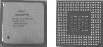
Figure 4.8: Pentium 4 (Northwood, Socket 478) processor
Pentium 4 (Northwood) processors have FC-PGA2 packaging with provisions for the Socket 478 processor slot (Fig. 4.9).
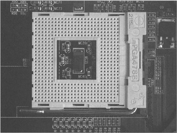
Figure 4.9: Socket 478 processor slot
Newer processor models intended for data-transfer rates of 533 MHz and 800 MHz have the C character in their markings and implement Intel's hyper-threading technology (Fig. 4.10). This technology allows the simultaneous execution of two tasks or two code sections of the same program on one physical processor. Thus, a single processor is interpreted by the OS as two logical devices operating in parallel. In two-processor systems, this technology allows work with four logical devices, and so on.
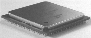
Figure 4.10: Pentium 4 3 GHz is intended to operate at a 200 MHz bus frequency, ensuring a data-transfer rate of 800 MHz
Tables 4.8–4.10 list the main temperature parameters of Pentium 4 (Northwood) processors, intended for operation at various bus frequencies and different core voltages set by VID. These processors can have the following VID values: 1.500 V, 1.525 V, and a multiple. The latter means that the exact VID setting can differ from the previous two values. It is set technologically, depending on the parameters of the processor chips being manufactured. For the models with a clock frequency to 2.8 GHz, the VID setting can take one of the following values: 1.475 V, 1.500 V, or 1.525 V. After overclocking, the VID setting can have one of the following values: 1.475 V, 1.500 V, 1.525 V, or 1.550 V.
|
Processor (GHz) |
Maximum thermal power (W) |
Maximum Tcase (°C) |
||||
|---|---|---|---|---|---|---|
|
VID=1.500 V |
VID=1.525 v |
VID=multiple |
VID=1.500 V |
VID=1.525 V |
VID=multiple |
|
|
2A |
52.4 |
54.3 |
54.3 |
68 |
69 |
69 |
|
2.2 |
55.1 |
57.1 |
57.1 |
69 |
70 |
70 |
|
2.4 |
57.8 |
59.8 |
59.8 |
70 |
71 |
71 |
|
2.5 |
59.3 |
61.0 |
61.0 |
71 |
72 |
72 |
|
2.6 |
- |
62.6 |
62.6 |
- |
72 |
72 |
|
Processor (GHz) |
Maximum thermal power (W) |
Maximum Tease (°C) |
||||
|---|---|---|---|---|---|---|
|
VID=1.500 V |
VID=1.525 V |
VID=multiple |
VID=1.500 V |
VID=1.525 V |
VID=multiple |
|
|
2.26 |
56.0 |
58.0 |
58.0 |
70 |
70 |
70 |
|
2.40B |
57.8 |
59.8 |
59.8 |
70 |
71 |
71 |
|
2.53 |
59.3 |
61.5 |
61.5 |
71 |
72 |
72 |
|
2.66 |
- |
66.1 |
66.1 |
- |
74 |
74 |
|
2.80 |
- |
68.4 |
68.4 |
- |
75 |
75 |
|
3.06 |
- |
- |
81.8 |
- |
- |
69 |
|
Processor (GHz) |
Maximum thermal power (W) |
Maximum Tcase (°C) |
|---|---|---|
|
2.4C |
66.2 |
74 |
|
2.6C |
69.0 |
75 |
|
2.8C |
69.7 |
75 |
|
3.0 |
81.9 |
70 |
With Pentium 4 processors based on the Northwood core, Intel released a Celeron processor line. As with models based on the Willamette core, these processors have 128 KB of L2 cache memory. Other parameters are similar to those of Pentium 4 (Northwood). The FSB clock frequency (100 MHz) and data-transfer rate (400 MHz) were inherited from the Celeron models based on the Willamette core (Table. 4.11).
|
Processor (GHz) |
Maximum thermal power (W) |
Maximum Tcase (°C) |
|---|---|---|
|
2.0 |
52.8 |
68 |
|
2.1 |
55.2 |
69 |
|
2.2 |
57.1 |
70 |
|
2.3 |
58.3 |
70 |
|
2.4 |
59.8 |
71 |
For processors based on the NetBurst microarchitecture, Intel developed special chipsets: i850 and i850E for two Rambus memory channels, i845 line for the SDRAM (PC133) and DDR SDRAM, and i875 and i865 for dual-channel DDR SDRAM. Appropriate chipsets also have been released by Via Technologies and SiS.
The next core for high-performance Intel processors for desktop PCs was named Prescott. As all earlier members of the Pentium 4 family, this core is based on the NetBurst microarchitecture.
This core has several innovations, including increased L1 and L2 cache memory, an improved mechanism of branch prediction, more efficient hyperthreading technology, and 13 new instructions known as PNI (Prescott New Instructions).
The new chip has about 100 million transistors. It is manufactured using 0.09-micrometer technology with so-called strained silicon.
Future models with the Socket 478 are anticipated. They, in turn, are expected to be replaced by models intended for Socket 775 LGA.
The next core, the successor of Prescott, will be Tejas.
AMD Athlon/Duron (Thunderbird/Spitfire)
AMD Athlon and AMD Duron processors are supplied in a PGA case. Motherboards supporting these processors have a special slot known as Socket A (462 pins) (Fig. 4.11).
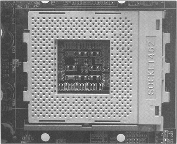
Figure 4.11: Socket A (462 pins) processor slot
Athlon is based on the Thunderbird core; Duron uses the Spitfire core.
Athlon processors are oriented toward powerful computers. The architecture of these processors includes 128 KB of L1 cache and 256 KB of L2 cache memory.
Duron processors were developed for relatively inexpensive computers. Their architecture differs from Athlon only in the amount of the L2 cache memory: 64 KB (Figs. 4.12 and 4.13).

Figure 4.12: Athlon (Thunderbird, Socket A) processor
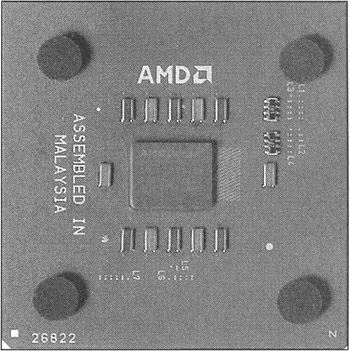
Figure 4.13: Duron (Spitfire, Socket A) processor
Both processor lines are intended to operate with the Alpha EV6 bus, designed by Digital Equipment Corp. (DEC) for its Alpha processors and licensed by AMD for its products. (The Alpha line is now a product of Hewlett-Packard.)
The Alpha EV6 bus, used as a processor bus (FSB), ensures data transmission on both fronts of the clock pulses (Double Data Rate). This increases the throughput, improving overall system performance. At 100 MHz, the Alpha EV6 FSB, usually named EV6, ensures data transfer at 200 MHz. In contract to EV6, the GTL+ and AGTL+ buses of Intel Celeron (Coppermine), Pentium II, and Pentium III processors have the same data rate and clock frequency.
Athlon and Duron processors require special motherboards with chipsets that support these processors. Such motherboards ensure stable operation of the processors, provided that sufficiently powerful power supply units are used. Usually, power supply units with a rating of no less than 235 W are recommended.
Athlon and Duron processors have significant technological reserve. Performance can be improved using overclocked modes that can be set, for example, by increasing the processor bus frequency.
Athlon and Duron, released in the PGA form factor, usually have fixed frequency multipliers. The form factor doesn't allow resistors to be changed, as in case with earlier specimens of Athlon. Therefore, frequency multipliers can be changed only by using specialized software and hardware.
The value of the frequency multiplier, relating internal and external processor frequencies, is set by the FID0-FID3 contacts. Supply voltage is set by VID0-VID4. Overclocking of such processors is easy: Most contemporary motherboards oriented toward these processors allow both the frequency multiplier and the core supply voltage of the processor to be changed. Some motherboards provide this functionality at the BIOS level (in BIOS Setup). Note that the processor core voltage can be increased no more than 10% above the nominal level. AMD's recommendations for specifying core supply voltages for Duron and Athlon are in Tables 4.12–4.14. This information changes with the release of new core implementations.
|
Processor |
Frequency (MHz) |
Minimum supply voltage (V) |
Standard supply voltage (V) |
Maximum supply voltage (V) |
|---|---|---|---|---|
|
Athlon |
650–850 |
1.60 |
1.70 |
1.80 |
|
900–1,000 |
1.65 |
1.75 |
1.85 |
|
|
Duron |
550–700 |
1.40 |
1.50 |
1.60 |
|
Minimum supply voltage (V) |
Standard supply voltage (V) |
Maximum supply voltage (V) |
|---|---|---|
|
1.65/1.70 |
1.75 |
1.80/1.90 |
|
Processor |
Frequency (MHz) |
Minimum supply voltage (V) |
Standard supply voltage (V) |
Maximum supply voltage (V) |
|---|---|---|---|---|
|
Athlon |
650–1,400 |
1.65 |
1.75 |
1.85 |
|
Duron |
600–950 |
1.50 |
1.60 |
1.70 |
Information on the power of Duron and Athlon, needed for precise analysis of the temperature mode and evaluation of the required cooling devices, is in Tables 4.15–4.19.
|
Processor frequency (MHz) |
Normal power (W) |
Maximum power (W) |
|---|---|---|
|
650 |
32.4 |
36.1 |
|
700 |
34.4 |
38.3 |
|
750 |
36.3 |
40.4 |
|
800 |
38.3 |
42.6 |
|
850 |
40.2 |
44.8 |
|
900 |
44.6 |
49.7 |
|
950 |
46.7 |
52.0 |
|
1,000 |
48.7 |
54.3 |
|
Processor frequency (MHz) |
Normal power (W) |
Maximum power (W) |
|---|---|---|
|
900 |
45.8 |
51.0 |
|
950 |
47.6 |
53.1 |
|
1,000 |
49.5 |
55.1 |
|
1,100 |
54.1 |
60.3 |


