3.1 Motherboard Characteristics
Several characteristics differentiate motherboards, including physical characteristics, which in combination are called the form factor; the chipset used, which defines the capabilities of the motherboard; the processors the motherboard supports; the BIOS it uses; and the internal and expansion busses that it supports. The following sections examine each of these factors.
3.1.1 Form Factor
Motherboards differ in size, shape, position of mounting holes, power supply connector type, and port types and locations. Together, these differences define the form factor of the motherboard. Form factor is a critical issue when you upgrade a system because the replacement motherboard must physically fit the case and use the existing power supply connectors. Form factor doesn't matter when you're building a new PC. You simply select the best motherboard for your needs, and then buy a case that fits it. Many motherboard manufacturers build similar motherboards in different form factors. Here are the form factors you may encounter:
- AT, Baby AT (BAT), and LPX
-
All of these form factors are based on the motherboard used in the original 1984 IBM PC AT and are obsolete. The most recent of these motherboards use chipsets and processors that are two or more generations out of date. Although a few such motherboards remain available, they are suitable only to replace failed motherboards in obsolete systems that for some reason must remain in service. Other than that, there is no good reason to buy one of these obsolete motherboards. A system that uses this form factor is too old to be economically upgradeable.
- ATX and variants
-
Nearly all current motherboards use the ATX form factor, or one of its smaller variants, the miniATX, mATX, FlexATX, and NLX. For a complete discussion of these form factors, including case and power supply issues, see Chapter 25 and Chapter 26.
- Proprietary
-
Although it is much less common nowadays to find new systems that use proprietary motherboards, such boards were relatively common a few years ago, particularly in systems sold by major manufacturers such as Compaq and IBM. A cynical observer might believe that the major manufacturers did this to lock customers in. In fact, it probably had more to do with the fact that the then-current Baby AT standard had reached the end of its useful life and the ATX standard had not yet become the obvious successor. To reduce manufacturing costs and increase reliability, manufacturers that had the in-house engineering talent to do so designed their own motherboards. Some of these are actually very elegantly designed. They all share one fatal flaw, however. They aren't standard. A system that uses a proprietary motherboard form factor is effectively not upgradeable.
|
3.1.2 Chipsets
Just as the motherboard defines a PC, the chipset defines a motherboard. The chipset determines the main characteristics of the motherboard?what processors it supports, what RAM types it can use, what bus types and speeds it supports, whether it supports standards such as AGP and USB, and so on. Chipsets are so named because they usually comprise two relatively large chips. Some chipsets contain three or more chips. A few chipsets, most of which are intended for low-cost systems, have all functions on one physical chip.
Figure 3-1 shows a block diagram for the 845PE, which until July 2003 was Intel's flagship chipset for the Pentium 4 and Celeron processors. Block diagrams are helpful in understanding the functions of a chipset. Like most chipsets, the 845PE comprises a Northbridge chip, labeled GMCH, and a Southbridge chip, labeled ICH4. The Northbridge interfaces the CPU, memory, and AGP video?all of which are high-bandwidth components. The Southbridge can conveniently be thought of as a peripheral controller. The Southbridge manages low- and moderate-bandwidth components such as the PCI bus, IDE interface, USB 2.0 ports, and so on. Some motherboards supplement Southbridge functions by adding another chip, often called a Super I/O controller.
Figure 3-1. Block diagram of the Intel 845PE chipset (graphic courtesy of Intel Corporation)
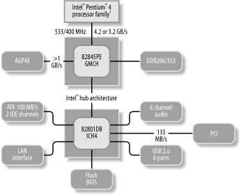
Chipset makers often use one Southbridge with different Northbridges to create chipsets for different processors. For example, Intel uses the 82801DB ICH4 Southbridge in numerous Pentium 4 and Celeron chipsets. It's also possible to use the same Southbridge to create chipsets for processors from different makers. For example, VIA Technologies produces chipsets for the Intel Pentium 4 and AMD Athlon?two processors with very different architectures?by combining the same Southbridge with a Northbridge that supports the processor in question.
|
There are scores of motherboard manufacturers, but only a handful of chipset manufacturers. This is because designing a chipset requires significant engineering resources, but building a motherboard around that chipset is straightforward. Chipset manufacturers want motherboard manufacturers to buy their chipsets, so they provide detailed specifications, engineering drawings, and reference samples, which make building motherboards more a matter of production than design.
If you examine 20 motherboards made by 20 different manufacturers, all using the same chipset, you'll find that the similarities outweigh the differences. There may be minor variations in features and layout, but the chief differences are the quality of the components used and the quality of construction. Accordingly, it is quite possible for one manufacturer to make a terrible motherboard and another manufacturer a superb motherboard, even though both use the same chipset. The motherboard market is so competitive that price is almost invariably an excellent predictor of the quality of a motherboard.
Understanding chipset basics is important whether you are upgrading an existing PC or building a new one. If you are upgrading, understanding the chipset tells you what can and cannot be done within its limitations. If you are building or buying a new PC, its chipset is the most important factor in determining motherboard performance and future upgradability. Understanding the differences between competing chipsets lets you make rational decisions about which computer or motherboard to buy. Because chipsets are so important, we've devoted a great deal of space to explain what you need to know about them.
3.1.2.1 CPU family support
Chipsets support only one of the following CPU families, because CPU families differ greatly in how they access and manage main memory, cache, and other major system components:
Intel Pentium Pro/Pentium II/Celeron/Pentium III sixth-generation CPUs
Intel Pentium 4/Celeron seventh-generation CPUs
AMD Athlon/Duron sixth-generation CPUs
AMD Hammer-series seventh-generation CPUs
A particular chipset may support most or all CPUs within a family, or may support only one of them. For example, some chipsets support the Pentium II, Celeron, and Pentium III CPUs, while others support only one or two of those. Also, chipsets designed for late variants within a generation may not support earlier variants within that generation. For example, Intel 815-family chipsets do not support the Pentium II and early variants of the Celeron. Similarly, Intel 875-family chipsets support the current Northwood- and Prescott-core Pentium 4, and will support the forthcoming Dothan-core Pentium 4 processors, but support neither the earlier Willamette-core Pentium 4 nor the Celeron.
3.1.2.2 CPU speed support
A chipset that supports a particular CPU may support all or only some of the speeds at which that processor is available. In general, faster CPUs require faster chipsets, so you might imagine that a chipset rated to handle the fastest version of a particular CPU could also handle slower versions of that CPU. That's not always the case, however. Modern motherboards accommodate different processor speeds by varying two settings, Front Side Bus (FSB) speed and CPU multiplier:
- FSB speed
-
FSB speed (also called host bus speed) specifies the speed at which the CPU communicates with the chipset. All sixth-generation and later chipsets support an FSB that runs at 66 MHz or faster, sometimes much faster. Early sixth-generation Intel chipsets use a 66 MHz FSB to support the Celeron and Pentium II processors. Later sixth-generation Intel chipsets use the 66 MHz and 100 MHz FSB to support Celeron, Pentium II, and Pentium III processors, and the 133 MHz FSB to support later Pentium III variants.
AMD Athlon chipsets introduced the concept of the double-pumped FSB, which transfers data on both the rising and falling sides of the clock pulse. Early Athlon chipsets supported the 66 MHz FSB double-pumped to 133 MHz, and the 100 MHz FSB doubled-pumped to 200 MHz. Later Athlon chipsets added support for FSB speeds of 133/266 MHz, 166/333 MHz, and 200/400 MHz.
Intel introduced the quad-pumped FSB in its seventh-generation Pentium 4 chipsets. First-generation Intel Pentium 4 chipsets used a 100 MHz FSB quad-pumped to 400 MHz. Later Intel chipsets increased the FSB to 133 MHz quad-pumped to 533 MHz, and the 200 MHz FSB quad-pumped to 800 MHz. Intel is careful to note that only data is transferred at the quad-pumped rate. Control instructions are transferred at half that rate, at 200 MHz on the 400 MHz FSB, 266 MHz on the 533 MHz FSB, and 400 MHz on the 800 MHz FSB. Still, because data comprises the vast bulk of what is transferred between processor and chipset, we consider Intel's FSB speed designations to be accurate.
For some motherboards, including many sixth-generation Intel and third-party motherboards, setting FSB speed also specifies the PCI bus speed. These motherboards, called synchronous motherboards, divide the FSB speed by a fixed factor to determine PCI bus speed. For a 100 MHz FSB, the divisor is 3.0, which runs the PCI bus at 33.3 MHz. A 133 MHz FSB uses a divisor of 4.0, which again runs the PCI bus at 33.3 MHz. Similarly, FSB speeds of 166 MHz and higher use divisors calculated to run the PCI bus at a standard 33.3 MHz.
Some motherboards, called asynchronous motherboards, allow FSB speed and PCI bus speed to be set independently, either by means of jumpers on the motherboard or by CMOS settings. They do this to allow using faster FSB speeds while limiting PCI bus speeds to 33 MHz, which is the fastest reliable setting for the standard 32-bit PCI bus. (64-bit and 66 MHz PCI slots are also available on some systems.) Otherwise, for example, overclocking a 100 MHz FSB processor by setting the FSB speed to 133 MHz would run the PCI bus at 44.4 MHz (one-third of 133), which is much too fast for reliability.
- CPU multiplier
-
specifies the multiple of FSB speed at which the CPU runs internally. Modern chipsets may support CPU multipliers from 3.0x to 10.0x or higher. For example, a 1200 MHz Pentium III/1.2G processor with a 133.33 MHz FSB uses a 9.0 multiplier, because 9.0 x 133.33 = 1200.0. Pentium 4 processors use a multiplier calculated against the underlying bus speed (100, 133, or 200 MHz) rather than the quad-pumped bus speed (400, 533, or 800 MHz). For example, a Pentium 4/2.4G processor with a 100/400 MHz FSB uses a 24x multiplier (24 x 100 MHz = 2.4 GHz). A Pentium 4/2.4G processor with a 133/533 MHz FSB uses an 18x multiplier, and a Pentium 4/2.4G with a 200/800 MHz FSB uses a 12x multiplier.
AMD names Athlon XP processors with model numbers rather than actual processor speed, but the same principle holds true. For example, an Athlon XP 3000+, which actually operates at 2.16 GHz, uses a 166/333 MHz FSB and a 13x CPU multiplier.
All recent AMD and Intel CPUs have a locked multiplier, which means the only way to run them faster than their rated speed is to set the FSB above nominal. For example, increasing the FSB to 150 MHz from the nominal 133 MHz for a Pentium III/1.2G runs the CPU at 1350 MHz (150 x 9.0). That results in a small performance increase, but also reduces system stability because the PCI bus is running at 37.5 MHz (150/4) rather than its design speed of 33.3 MHz and because other system components are being pushed beyond their design limits.
Not all motherboards allow these parameters to be controlled manually. Some motherboards, including many early sixth-generation Intel models, allow you to set only CPU speed, which in turn selects a predetermined combination of memory bus speed and CPU multiplier. This is done to prevent overclocking, or running the CPU at higher than its rated speed, a practice that Intel naturally discourages. Late sixth-generation and seventh-generation Intel motherboards have no user-accessible speed settings at all, depending on the CPU to identify itself to the motherboard and setting the FSB speed and CPU multiplier accordingly. AMD, which was formerly relatively "overclocking-friendly" has also taken steps to lock down its CPUs to prevent casual overclocking.
Other motherboards, including third-party models that support Intel sixth-generation CPUs, may provide a means to set both FSB speed and CPU multiplier, either by means of a jumper setting or a menu selection in BIOS Setup. Setting CPU multipliers manually is ineffective for nearly all Intel sixth-generation and later processors, all AMD Duron processors, and all Socket A Athlon processors because they use multiplier locks.
|
FSB speeds, on the other hand, are externally determined and not locked, although Intel has recently begun efforts to lock FSB speeds as well. That means that at least for now you can change the processor speed by setting the FSB speed to some value other than nominal, assuming that the motherboard gives you that option. For example, a 1.2 GHz AMD Athlon is designed to operate with a 133 MHz FSB speed and a 9.0x multiplier. There's nothing you can do to boost the multiplier (short of getting out your pencil), but you can set the FSB speed to a faster value?say, 140 MHz. That causes the processor to run at 1260 MHz rather than 1200 MHz, a gain so minor that it will not be noticeable.
|
3.1.2.3 Memory bus speed and width
One of the primary functions of a chipset is to serve as an intermediary between the processor and main memory. The memory controller portion of the chipset has two important duties. First, it reduces load on the processor by performing some memory functions without intervention from the processor, including routine housekeeping chores such as refreshing memory and managing DMA. Second, when the processor reads from or writes to main memory, it does not do so directly. Instead, the memory controller portion of the chipset works as the middleman, accepting data from the processor and transferring it to main memory, or vice versa.
Just as the FSB connects the chipset to the processor, the memory bus connects the chipset to main system memory. The speed and width of the memory bus determine how fast data can be transferred between the chipset and main memory. Unless the memory bus can transfer data at least as fast as the FSB can, the processor may become starved for data. Accordingly, modern chipsets are optimized to provide a fast memory bus. The following two interrelated factors determine throughput:
- Memory bus speed
-
Memory bus speed determines the fastest memory that can be used. For example, a chipset may be designed to support DDR-SDRAM at a maximum memory bus speed of 333 MHz, which means that the memory bus is optimized for DDR333 (PC2700) memory. Another chipset may be designed to use DDR-SDRAM at a maximum memory bus speed of 400 MHz, which means that the memory bus is optimized for DDR400 (PC3200) memory. A fast memory bus can use slower memory. For example, a chipset that supports PC3200 memory can typically use PC2700 memory instead. A slower memory bus can use faster memory, but the speed of the memory bus limits the memory to operating slower than its rated speed. For example, a system whose chipset supports at most PC2700 memory can use PC3200 memory, but treats it as though it were PC2700 memory. Sixth- and seventh-generation chipsets use memory bus speeds that range from 66 MHz to 400 MHz.
- Memory bus width
-
Standard SDR-SDRAM and DDR-SDRAM chipsets use a 64-bit (8-byte) wide memory path. The product of bus speed and bus width determines the maximum peak throughput available. For example, a 64-bit memory bus running at 400 MHz can transfer up to 8 bytes x 400 MHz, or 3200 MB per second. Some sixth- and seventh-generation chipsets support a dual-channel memory bus, which doubles the memory bus width, thereby transferring twice as much data per clock cycle. For example, the nVIDIA nForce2 and Intel 875P chipsets support dual-channel DDR-SDRAM at 400 MHz, which provides throughput of 16 bytes per transfer at 400 MHz, or 6400 MB per second.
In an ideal system, the memory throughput matches the processor bandwidth. For example, the Pentium 4 communicates data 64 bits (8 bytes) at a time. For a Pentium 4 with an 800 MHz FSB, the processor bandwidth is (8 bytes x 800 MHz), or 6400 MB/s. Dual-channel PC3200 DDR-SDRAM also has throughput of 6400 MB/s, and is therefore an ideal match for this processor. Conversely, an AMD Athlon with a 333 MHz FSB has a bandwidth of (8 bytes x 333 MHz), or 2667 MB/s, and so is a perfect match for a single-channel PC2700 DDR-SDRAM memory controller. Table 3-1 lists the minimum memory throughput necessary for a balanced configuration at various FSB speeds.
|
FSB speed |
CPU bandwidth |
Minimum balanced memory configuration |
|---|---|---|
|
100 |
800 MB/s |
single-channel PC100 SDR |
|
133 |
1067 MB/s |
single-channel PC133 SDR |
|
200 |
1600 MB/s |
single-channel PC1600 DDR |
|
266 |
2133 MB/s |
single-channel PC2100 DDR |
|
333 |
2667 MB/s |
single-channel PC2700 DDR |
|
400 |
3200 MB/s |
single-channel PC3200 DDR |
|
533 |
4267 MB/s |
dual-channel PC2100 DDR |
|
800 |
6400 MB/s |
dual-channel PC3200 DDR |
This balance between processor bandwidth and memory bus throughput explains why some processors benefit greatly from a faster memory bus, and others benefit little or not at all. For example, a 133 MHz FSB Pentium III has processor bandwidth of only 1067 MB/s, which means that using memory faster than PC133 SDR-SDRAM will not increase system performance because processor bandwidth becomes the bottleneck. Similarly, because no AMD Athlon processor uses an FSB faster than 400 MHz, there is little benefit in using a dual-channel memory controller with an Athlon.
Lack of balance also explains why a particular processor may perform better on one chipset than on another. For example, consider a 533 MHz FSB Pentium 4. When that processor is used with an Intel 875P chipset (dual-channel PC2700 or PC3200 DDR-SDRAM), the memory bus is more than fast enough to keep up with the 4267 MB/s bandwidth of the processor. But if that 533 MHz FSB processor is used on an Intel 845PE chipset (single-channel PC2700 DDR-SDRAM), the 4267 MB/s bandwidth of the processor is much higher than the 2667 MB/s throughput of the memory bus. Accordingly, during memory-intensive operations the processor may have to wait for memory to supply data.
The memory controllers in some chipsets link memory bus speed to FSB speed. Even though the chipset may support faster memory and you may have faster memory installed, the memory runs at the lower speed determined by the FSB speed. For example, a Pentium 4 chipset that supports PC2100, PC2700, and PC3200 DDR-SDRAM memory may allow you to use only the PC2100 memory bus speed with a 400 MHz FSB processor (regardless of the actual speed of the memory installed). With a 533 MHz FSB processor, that chipset may allow you to use either the PC2100 or PC2700 memory bus speed, and with an 800 MHz FSB processor, only the PC3200 speed.
Conversely, the memory controllers in some chipsets allow the memory bus speed to be set independently of the FSB speed. For example, the nVIDIA nForce2 chipset allows using PC3200 memory running at full speed regardless of the FSB speed of the installed processor. Although that may seem to be advantageous, the reality is that it seldom makes any difference.
When our ASUS A7N8X Deluxe motherboard sample arrived, we jumped on it because for the first time we'd be able to test the effect of different FSB and memory bus speeds, as well as the effect of dual-channel versus single-channel memory. What we found didn't surprise us. The benefit of dual-channel versus single-channel memory was nearly nil. We expected that because single-channel PC2100 or PC2700 memory is fast enough for the 266 MHz and 333 MHz Athlon FSBs, respectively.
Even with the 333 MHz FSB Athlon, dual-channel memory showed almost no improvement over single-channel, nor did PC3200 memory run any faster than PC2700, at least within the limits of error for our benchmark tests. If anything, the PC3200 memory was slower than PC2700 memory in this configuration, and that brings up an interesting point.
It's obviously bad to use memory that has lower throughput than the processor bandwidth because the memory can't keep up with the demands of the processor. Less obvious, but just as important, it can be bad to use memory that has a higher throughput than processor bandwidth. Why? Because mismatching FSB speed and memory bus speed requires the chipset to buffer transfers between main memory and the processor. Although chipset designers do everything possible to minimize the overhead costs of such buffering, there is still a price to be paid. The upshot, as we found, is that using a memory bus speed faster than what the processor requires can actually reduce memory performance.
3.1.2.4 Multiple CPU support
Some chipsets support motherboard configurations with multiple CPU sockets. These chipsets coordinate operations between the multiple processors and memory, which is necessary but not sufficient to allow symmetric multiprocessing (SMP) operation. In addition to chipset support, SMP requires:
- CPU SMP support
-
Non-Intel CPUs other than the AMD Athlon and Duron lack the circuitry to support SMP. Intel fifth- and sixth-generation CPUs support SMP, except Coppermine128-core or later Celerons and most Coppermine-core Pentium IIIs at 1 GHz and faster. The Pentium 4 does not support SMP except in its more expensive Xeon variant. AMD produces a special version of the Athlon called the Athlon MP that supports SMP applications in conjunction with the AMD-760MP or AMD-760MPX chipset.
- Operating system SMP support
-
DOS, Windows 3.X, and Windows 9X do not support SMP. Running one of these operating systems on an SMP PC uses only one of the CPUs. Windows NT/2000/XP Pro supports SMP, as do most Intel-based Unix implementations, including Linux. Note that Windows XP Home does not support SMP.
If you run an SMP-aware operating system, consider buying a motherboard that supports dual CPUs. The incremental cost is generally small, and the increased performance is significant. Prior to 2001, Intel's pricing strategy often made buying two midrange Pentium III processors less expensive than buying one top-of-the-line Pentium III. Although the AMD Athlon and Duron processors were inherently dual-capable, no SMP chipset existed for them. As a result, many enthusiasts built dual-processor Pentium III systems.
That changed when AMD shipped the dual-capable 760MP chipset, and followed not long after with the enhanced 760MPX SMP chipset. Suddenly, it became possible to build an inexpensive, fast dual-AMD system. At the same time, Intel de-emphasized entry-level SMP systems by replacing the SMP-capable i440BX chipset with newer sixth-generation chipsets that did not support SMP, and by removing SMP support from later Pentium III variants as well as from the mainstream Pentium 4 processors.
Alas, AMD has not updated the 760MPX chipset to add support for features such as USB 2.0, Serial ATA, PC2700 and PC3200 memory, and so on. Although the 760MPX platform remains a cost-effective platform with reasonably high performance, it is beginning to show its age. At the same time, Intel supports SMP only in its high-end chipsets and with Xeon processors, which makes the cost of an Intel dual-processor solution higher than it used to be.
Fortunately, the pricing gap between Intel dual-capable Xeon processors and dual-capable Athlon processors has recently narrowed, albeit in part because AMD increased the price of its dual-capable processors by introducing the Athlon MP line of processors certified for dual operation. Xeon processors are now priced competitively against Athlon MP processors, but alas, the days of using a pair of $75 processors in a dual rig are gone. Nowadays, if you want a dual-processor system, it's going to cost you. You must buy premium-priced Xeon or Athlon MP processors, or risk using uncertified Athlon XP processors for dual operation. Rats.
|
3.1.2.5 I/O bus support
The chipset determines what I/O bus standards the motherboard can support. The chipset manages the I/O busses, arbitrating data transfer between them, the CPU, and system memory. The chipset features determine which I/O busses the system supports, the speed at which the busses operate, and what additional related system features are supported. Depending on how you count, half a dozen or more I/O bus standards have been in common use since the first PCs. In order of their appearance, they include:
- Industry Standard Architecture (ISA)
-
Used in 8-bit form in the PC and XT and 16-bit form in the PC/AT. Obsolete, but most motherboards made through 2000 provided at least one ISA slot for legacy cards. By late 2000, many new motherboard models shipped without ISA slots. Good riddance, we say.
- MicroChannel Architecture (MCA)
-
An IBM standard that never caught on. Obsolete.
- Extended Industry Standard Architecture (EISA)
-
An open standard developed by Compaq and eight other PC makers (the so-called "Gang of Nine") to compete with the proprietary MCA, but which achieved only limited acceptance, primarily in servers. Obsolete.
- VESA Local Bus (VLB)
-
An open standard that was widely used in 486 systems, but whose technical shortcomings made it inappropriate for Pentium and later systems. Obsolete.
- Peripheral Component Interconnect (PCI)
-
An open standard developed by Intel, used on late-model 486 systems and almost universally for Pentium and later systems. Older PCI systems use the PCI 2.0 standard, which limits upgrade possibilities. Newer motherboards use PCI 2.1, and current models use PCI 2.2. The PCI 2.3 Specification was approved in summer 2001, but products based on that standard are just now beginning to be deployed. PCI 3.0 was originally intended to be finalized in 2002, but various issues have delayed that standard, and we do not expect to see PCI 3.0 products until at least 2004.
- Accelerated Graphics Port (AGP)
-
A dedicated I/O port used on late-model fifth-generation and most sixth- and seventh-generation motherboards to provide high-performance graphics. Not technically a bus because it supports only one device, but thought of as a bus because it is implemented as an expansion slot. Note that many current motherboards support only AGP 2.0 1.5V and/or AGP 3.0 0.8V video adapters, and cannot accept legacy 3.3V AGP video adapters. For complete details about AGP, see Chapter 15.
Older motherboards provide a mix of expansion slots, usually four or five PCI slots and one shared ISA/PCI slot that can accept either type of expansion card. The chipset provides bridging functions between these I/O busses (the PC-to-ISA bridge) and between I/O busses and other system busses, including the memory bus. Current motherboards have no ISA slots at all, and contain only PCI slots and perhaps an AGP slot.
3.1.2.6 Embedded feature support
The chipset also provides various embedded low-level system functions and features. Many low-level system functions?e.g., the PIC?are well-standardized and have been so for years, so there is little to choose from among different chipsets on that basis. But features differ between chipsets, not so much between competing chipset models as between generations. Chipsets of the same generation generally implement similar features in comparable ways, so these are not issues for choosing between current chipsets. The following features are important when evaluating the upgradability of a motherboard that uses an older chipset:
- ATA interface
-
Any modern motherboard provides an embedded dual-channel ATA/ATAPI interface, which supports a total of four ATA/ATAPI devices, two per channel. But not all embedded ATA interfaces are equal. All current motherboards support ATA/100, and some support the ATA/133 standard, which has been rendered moot by the Serial ATA standard. The fastest current hard disks at peak throughput can barely saturate an ATA/66 interface, but choosing a chipset that supports at least ATA/100 makes hard disk upgrades easier. If you are upgrading a system with an old motherboard, the chipset should support at least PIO-4 and independent device timing, which allows two dissimilar devices on one channel to both run at their optimal speed. If you are upgrading a system that uses an otherwise suitable older motherboard that does not support these features, you can disable the embedded ATA interface and install an ATA expansion card that supports recent ATA standards.

The current ATA standard specifies 28-bit addressing, which places an absolute upper limit of 128 GB on ATA drives that use the standard 512 bytes/sector. The Maxtor Big Drive Initiative extends ATA addressing to 48 bits, which allows drive sizes of up to 128 PB, which is to say a binary million times larger than the current limit. This initiative is backed by other major industry players, including Microsoft, and has been incorporated in the new ATA standard. The most recent motherboards support 48-bit LBA natively, although some do so only for SATA ports. Motherboards based on chipsets more than a year old typically do not support 48-bit LBA for parallel ATA interfaces. However, inexpensive PCI adapters are available from vendors such as Promise Technology and SIIG that allow retrofitting 48-bit LBA PATA drives into existing systems. All SATA interfaces, embedded or add-on, support 48-bit LBA.
- DMA controller and DMA mode support
-
Direct Memory Access (DMA) is a means to transfer data between devices without using the CPU as an intermediary, which can increase system performance. For example, a hard drive can use DMA to transfer data to and from memory without passing it through the CPU, allowing the CPU to do other things at the same time. DMA can be implemented using the DMA controller on the motherboard itself (called first-party DMA) or by using a DMA controller embedded on a device (called third-party DMA or bus mastering DMA). Older chipsets provide a limited selection of slower DMA modes and may make DMA available only on some expansion slots, which are typically differentiated by being a different color than non-DMA slots. Newer chipsets provide additional DMA modes, faster DMA transfers, and DMA capability on all expansion slots.
- Plug and Play (PnP) support
-
The PnP standard is closely linked to the PCI standard. Systems that have chipsets, BIOSs, peripherals, and operating systems that are PnP-aware recognize and configure installed hardware automatically, eliminating IRQ, I/O base address, and DMA resource conflicts. A system that uses a non-PnP chipset is too old to upgrade effectively other than by replacing the motherboard.
- Universal Serial Bus (USB) support
-
USB will eventually replace legacy I/O port standards, including serial, parallel, keyboard, and mouse ports. Most motherboards shipped since 1996 use chipsets that are USB 1.0- or 1.1-compliant. All current chipsets include USB support, and those designed from late 2002 onward support the USB 2.0 standard, which increases maximum data rates forty-fold to 480 Mb/s. To add USB 2.0 support to an older system, install an inexpensive PCI USB 2.0 card, such as those available from Adaptec, Belkin, SIIG, and many others.
You may have USB ports you don't know about. Many motherboards have "extra" USB ports that appear only as sets of header pins on the motherboard. Using these ports requires adding a port extender to route USB signals from the header pins to the outside of the case, usually to the back panel. Some newer cases have front-accessible USB connectors, which make it much easier to connect and disconnect USB devices that are moved frequently, such as cameras. We generally connect "permanent" USB devices such as printers and scanners to the USB ports on the back panel, and reserve front-panel USB ports for devices that we connect and disconnect frequently.
- Accelerated Graphics Port (AGP) support
-
AGP provides a fast, dedicated channel between the CPU and an AGP video adapter, moving video data off the memory bus. Because AGP is implemented as an expansion slot, any AGP-capable motherboard by definition uses an AGP-capable chipset and provides an AGP slot. But the AGP standards specifies different modes, including 1X, 2X, 4X, and 8X, not all of which are implemented in all chipsets. AGP 1X is obsolete, although you can use an AGP 2X or 4X adapter in an AGP 1X motherboard. Most current motherboards support only 1.5V AGP 4X and/or 0.8V AGP 4X/8X adapters. The additional potential throughput of 4X is of little or no benefit with current video adapters, few of which can saturate even 2X AGP. Motherboards that support 8X AGP began shipping in late 2002, although once again the additional potential throughput of AGP 8X is not used by any current adapter. A few motherboards, most of which are intended for workstations, have an AGP Pro slot. AGP Pro is a backward-compatible extension of AGP that provides the additional power needed by some very high-performance video cards. Unless you plan to install an AGP Pro video adapter, you have no need for AGP Pro. When you buy a motherboard, make sure it supports at least AGP 4X. AGP 8X support is good in the sense that it means the chipset is up to date. Any motherboard that doesn't support at least 1.5V AGP 4X is out of date.
3.1.2.7 Identifying chipsets
To make upgrade decisions based on chipset, you must identify which chipset you have. If you are buying a new motherboard, this is straightforward. The motherboard specifications always list the chipset. When you upgrade an existing system, determining which chipset it uses can be difficult. You can identify the chipset in one of the following ways:
If you have the documentation for the system board or the PC, the chipset it uses will be listed in the detailed specifications. If you do not have the documentation, but can identify the make and model of the PC or motherboard, the manufacturer's web site should list the chipset it uses.
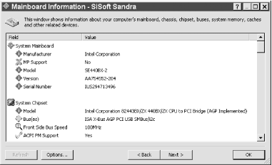
Use a third-party diagnostics program such as Smith Micro CheckIt or SiSoft Sandra to display system information. Figure 3-2 shows the results of running Sandra on an old Pentium III system. If you have no documentation, using a diagnostic utility is by far the easiest way to identify the chipset.
Figure 3-2. SiSoft Sandra identifying the chipset as an Intel 440BX
Many Windows diagnostics programs do not run or have limited functionality under Windows NT/2000/XP, which limit access of applications to underlying hardware. Although Windows utilities such as Sandra provide useful information, they cannot fully test or report on low-level system hardware resources. If you need to run comprehensive testing and diagnostics on an NT/2000/XP system, the best alternative is to boot a DOS- or Linux-based diagnostic utility from floppy disk or CD.
If you are running Linux, open a terminal, change to the /proc directory, type the command cat pci, and examine the listing for the Host Bridge, which should be the first item. The following excerpt shows part of the /proc/pci file for a system running an Intel 845 chipset:
PCI devices found:
  Bus  0, device   0, function  0:
    Host bridge: Intel Corp. 82845 845 (Brookdale) Chipset Host Bridge \
       (rev 4).
Identify the chipset visually by examining the motherboard. Most chipsets have two chips, although some have only one and a few have three or more. Look for relatively large, usually square chips that are labeled with the name of a chipset manufacturer?Intel, VIA, SiS, ALi, Opti, etc. Record the string of numbers and letters that identifies each such chip. Then visit that manufacturer's web site and search for those strings to determine which chipset, if any, those chips belong to. For example, if you locate an Intel chip labeled 82438VX, a quick check of the Intel web site tells you that that chip is part of an Intel 430VX chipset (Intel calls most of its recent chipset models a PCIset or an AGPset). Note, however, that, particularly on recent systems, whose chipsets run at very high speeds, the chips that make up the chipset may have permanently installed heatsinks, which makes it impossible to read the labels.
3.1.2.8 Fifth-generation chipsets
Systems that use fifth-generation (Pentium) chipsets are too old to be economically upgradeable. Even if such a system is technically upgradeable, it is not cost-effective to do so. Instead, retire that system in situ to less-demanding duties, and build a new system based on current technology.
3.1.2.9 Sixth-generation Intel and Intel-compatible chipset characteristics
Intel has produced numerous sixth-generation chipsets in the 4-series and 8-series lines. Table 3-2 lists the characteristics of Intel 4-series desktop chipsets. These chipsets are obsolescent, although systems built on them may still be used productively and may even be reasonable upgrade candidates. In fact, motherboards based on the 440BX chipset were still produced as recently as late 2002, and motherboards based on i815-series chipsets were in current production as of July 2003. Although systems based on these chipsets lack modern features, they remain useful for some applications.
|


