4.3 AMD Processors
Until late 1999, Intel had the desktop processor market largely to itself. There were competing incompatible systems such as the Apple Mac, based on processors from Motorola, IBM, and others, but those systems sold in relatively small numbers. Some companies, including Cyrix, IDT, Harris, and AMD itself, made Intel-compatible processors, but those were invariably a step behind Intel's flagship processors. When those companies?which Intel calls "imitators"?were producing enhanced 286s, Intel was already shipping the 386 in volume. When the imitators began producing enhanced 386-compatible processors, Intel had already begun shipping the 486, and so on. Each time Cyrix, AMD, and the others got a step up, Intel would turn around and release its next-generation processor. As a result, these other companies' processors sold at low prices and were used largely in low-end systems. No one could compete with Intel in its core market.
All of that changed dramatically in late 1999, when AMD began shipping the Athlon processor. The Athlon didn't just match the best Intel processors. It was faster than the best Intel could produce, and was in many respects a more sophisticated processor. Intel had a fight on its hands, and it does to this day.
If you ever take a moment to appreciate how much processor you can get for so little money nowadays, give thanks to AMD. Without AMD, we'd all still be running sixth-generation Intel processors at 750 MHz or so. An entry-level Intel processor would cost $200 or $250, and a high-end one (that might run at 1 GHz) would probably cost $1,000 or more. The presence of AMD as a worthy competitor meant that Intel could no longer play the game of releasing faster processors in dribs and drabs at very high prices. Instead, Intel had to fight for its life by shipping faster and faster processors at lower and lower prices. We all have AMD to thank for that, and Intel should thank AMD as well. Although we're sure Intel wishes AMD would just disappear (and vice versa), the fact is that the competition has made both Intel and AMD better companies, as well as providing the obvious benefits to us, the users.
The following sections describe current and recent AMD processor models.
4.3.1 The AMD Athlon Family
The AMD Athlon, which was originally code-named the K7 and began shipping in August 1999, was the first Intel-compatible processor from any maker that could compete on an equal footing with mainstream Intel processors of the time. First-generation Athlon processors matched or exceeded Katmai-core Pentium III processors in most respects, including (for the first time ever) floating-point performance. Intel finally had a real fight on its hands.
Although AMD represented the Athlon as the first seventh-generation processor, we regard the K7 Athlon as essentially an enhanced sixth-generation processor. Athlon has, in theory, several advantages relative to the aging Intel sixth-generation architecture, including the ability to perform nine operations per clock cycle (versus five for the Pentium III); more integer pipelines (three versus two); more floating-point pipelines (three versus one); a much larger L1 cache (128 KB versus 32 KB); more full x86 decoders (three versus one); and a faster FSB (100 MHz double-pumped to 200 MHz by transferring data on both the rising and falling edges of the clock cycle versus the single-pumped Intel 100/133 MHz bus, which transfers data only once during a clock cycle). While all that was very nice, tests showed that in practice the K7 Athlon and Pentium III were evenly matched at lower clock speeds, with the Pentium III sometimes showing a slight advantage in integer performance, and the Athlon a slight advantage in floating-point performance. At higher clock speeds, however, where the Pentium III L2 cache running at full CPU speed comes into play, the Coppermine Pentium III won most benchmarks handily.
AMD produced two variants of the first-generation Athlon, both in Slot A form. The earliest Athlons used the 0.25m K7 core, but AMD transitioned within a few months to the improved 0.18m K75 core, which was code-named Pluto for speeds lower than 1 GHz and Orion in the 1 GHz model. Although the K7 and K75 Athlons were good processors, they had the following drawbacks:
- Poor chipset and motherboard support
-
Initial acceptance of the Athlon was hampered because the only chipset available was the AMD-750, which was originally intended as a technology demonstrator rather than as a production chipset. The VIA KX133 chipset, originally planned to ship at the same time as the Athlon, was significantly delayed, and motherboards based on the KX133 began shipping in volume only in the second quarter of 2000. Many motherboard manufacturers delayed introducing Athlon motherboards, and their first products were crude compared to the elegant motherboards available for the Pentium III. In addition to indifferent quality, stability, compatibility, performance, and features, first-generation Athlon motherboards were in short supply and relatively expensive compared to comparable models for the Pentium III. In addition, KX133-based motherboards had problems of their own, including their inability to support Slot A Thunderbird-core Athlons. AMD soon made it clear that Slot A was an interim solution and that it would quickly transition to Socket A, so manufacturers devoted little effort to improving orphaned Slot A motherboards.
- Fractional CPU-speed L2 cache
-
Like the Deschutes-core Pentium II and the Katmai-core Pentium III, K7 Athlons run L2 cache at half CPU speed. Unlike the Coppermine Pentium III, which uses on-die L2 cache running at full CPU speed, the Athlon uses discrete L2 cache chips, which AMD had to buy from third parties. The Athlon architecture allows running L2 cache at anything from a small fraction of CPU speed to full CPU speed. AMD took advantage of this as it introduced faster versions of the Athlon by reducing the speed of L2 cache relative to processor speed, allowing the company to use less expensive L2 cache chips. The Athlon/700 and slower run L2 cache at 1/2 CPU speed; The Athlon/750, /800, and /850 run L2 cache at 2/5 CPU speed. the Athlon/900 and faster run L2 cache at 1/3 CPU speed. Unfortunately, compared to the full-speed Pentium III Coppermine L2 cache, the slow L2 cache used on fast Athlons decreases performance substantially in many applications.
- High power consumption
-
Early Athlon processors were power-hungry, with some 0.25m models consuming nearly 60 watts. In comparison, typical Intel processors used one-half to one-third that amount. High power consumption and the resulting heat production had many implications, including the requirement for improved system cooling and larger power supplies. In fact, for the Athlon, AMD took the unprecedented step of certifying power supplies for use with its processor. If you built a system around a first-generation Athlon, you had to make sure that both cooling and power supply were adequate to meet the extraordinarily high current draw and heat dissipation of the processor.
- Lack of SMP support
-
Until mid-2001, no multiprocessor Athlon systems existed. Although all Athlon processors from the earliest models have been SMP-capable (and in fact use the superior point-to-point SMP method rather than Intel's shared bus method), dual-processor Athlon systems had to wait for the release of the AMD-760MP chipset (originally designated the AMD-770) in mid-2001. This early absence of SMP support hurt Athlon acceptance in the critical corporate markets, not so much because there was a huge demand for SMP but because the lack of SMP support led buyers to consider the Athlon a less advanced processor than Intel's offerings.
With the exception of SMP support, which was never lacking in the processor, these faults were corrected in the second generation of Athlon CPUs, which are based on the enhanced K75 core code-named Thunderbird. All early Athlon models used Slot A, which is physically identical to Intel's SC242 (Slot 1), but uses EV-6 electrical signaling rather than the GTL signaling used by Intel. Figure 4-10 shows a Slot A Athlon processor.
Figure 4-10. AMD Slot A Athlon processor
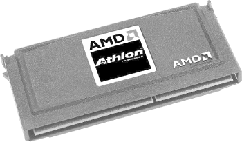
Table 4-3 lists the important characteristics of first- and second-generation Slot A Athlon variants (Model 3 is missing because it was assigned to the Duron processor). All Slot A variants use the double-pumped 100 MHz FSB, for an effective 200 MHz FSB speed. First-generation (K7- and K75-core) Athlons are characterized by their use of 512 KB L2 cache running at a fraction of CPU speed and by their use of split core and I/O voltages. Second-generation (Thunderbird-core) Athlons are characterized by their use of a smaller 256 KB L2 cache that operates at full CPU speed and by the elimination of split voltages for core and I/O. Thunderbird processors were produced in very small numbers in Slot A for OEM use, and so are included in this table for completeness, but we've never actually seen a Slot A Thunderbird and don't know anyone who has.
|
Athlon |
Athlon |
Athlon |
Athlon |
Athlon |
Athlon | |
|---|---|---|---|---|---|---|
|
Core |
K7 |
K75 |
K75 |
K75 |
Thunderbird |
Thunderbird |
|
Model |
1 |
2 |
2 |
2 |
4 |
4 |
|
Production dates |
1999, 2000 |
2000 |
2000 |
2000 |
2000, 2001 |
2000, 2001 |
|
Clock speeds (MHz) |
500, 550,600, 650, 700 |
550, 600,650, 700 |
750, 800,850 |
900, 950, 1000 |
700, 750, 800, 850 |
900, 950,1000 |
|
L2 cache size |
512 KB |
512 KB |
512 KB |
512 KB |
256 KB |
256 KB |
|
L2 cache speed |
1/2 CPU |
1/2 CPU |
2/5 CPU |
1/3 CPU |
CPU |
CPU |
|
L2 cache bus width |
64 bits |
64 bits |
64 bits |
64 bits |
64 bits |
64 bits |
|
System bus speed |
200 MHz |
200 MHz |
200 MHz |
200 MHz |
200 MHz |
200 MHz |
|
Core voltage |
1.6 |
1.6 |
1.6 (750) 1.7 (800/850) |
1.8 |
1.7 |
1.75 |
|
I/O voltage |
3.3 |
3.3 |
3.3 |
3.3 |
1.7 |
1.75 |
|
Dual CPU-capable |
m |
m |
m |
m |
m |
m |
|
Fabrication process |
0.25m |
0.18m |
0.18m |
0.18m |
0.18m |
0.18m |
|
Interconnects |
Al |
Al |
Al |
Al |
Al/Cu |
Al/Cu |
|
Die size (mm2) |
184 |
102 |
102 |
102 |
120 |
120 |
|
Transistors (million) |
22 |
22 |
22 |
22 |
37 |
37 |
Like Intel, which shifted from Slot 1 to Socket 370 for low-end processors, AMD recognized that producing cartridge-based slotted processors was needlessly expensive for the low end, and made it more difficult to compete in the value segment. Also, improvements in fabrication made it possible to embed L2 cache directly on the processor die rather than using discrete cache chips. Accordingly, AMD developed a socket technology, analogous to Socket 370, which it called Socket A. AMD had never denied that Slot A was a stopgap technology, and that Socket A was its mainstream technology of the future. AMD rapidly phased out Slot A during 2000, and by late 2000 had fully transitioned to Socket A. AMD has to date produced four major Athlon variants in Socket A. From earliest to latest, these include:
- Athlon (Thunderbird core)
-
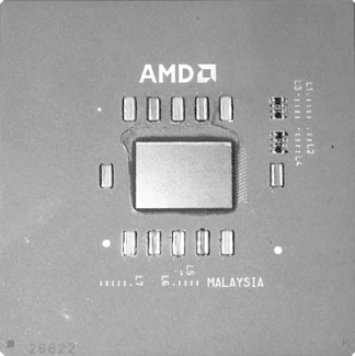
The Thunderbird Athlon was originally designated Athlon Professional and targeted at the mainstream desktop and entry-level workstation market, in direct competition with the Intel Pentium III and Pentium 4. The first Thunderbird processors used an 0.18m process with aluminum interconnects, but by late 2000 AMD had transitioned to a 0.18m process with copper interconnects. During that transition, AMD phased out Slot A Thunderbird models, and shifted entirely to Socket A. Early Thunderbirds used the 100 MHz FSB (double-pumped to 200 MHz), with later models also available in 133 MHz FSB variants. Figure 4-11 shows a Socket A Athlon Thunderbird processor.
Figure 4-11. AMD Socket A Athlon Thunderbird processor

There was to have been another variant of the Thunderbird-core Athlon, code-named Mustang and formally named Athlon Ultra, but that processor shipped only as samples. Mustang was to be a Socket A part, targeted at servers and high-performance workstations and desktops. It was to be an enhanced version of Thunderbird, with reduced core size, lower power consumption, and large, full-speed, on-die L2 cache, probably 2 MB or more. Mustang was to have used a 133 MHz DDR FSB, yielding an effective FSB of 266 MHz. It was intended to use a 0.18m process with copper interconnects from the start, and to require the AMD-760 chipset or later. Alas, the Mustang never shipped. It would have been a wonderful processor for its time.
- Athlon XP (Palomino core)
-
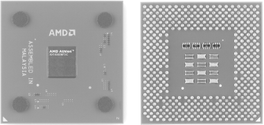
AMD originally intended to name the Palomino-core Athlon the Athlon 4, for obvious reasons. In fact, the first Palomino-core Athlons that shipped were the Mobile Athlon 4 and the 1.0 GHz and 1.2 GHz versions of the Athlon MP. Instead, given Microsoft's schedule for introducing Windows XP, AMD decided its new processor might tag along on the coattails of the new Windows version. Accordingly, AMD finally named the Palomino-core Athlon the Athlon XP. Various architectural changes from the Thunderbird core, detailed later in this section, allow the Athlon XP to achieve considerably higher performance at a given clock speed than a comparable Thunderbird. The Athlon XP is also the first recent AMD processor to use a model designation unrelated to its actual clock speed. All Palomino-core Athlons use the 133/266 MHz FSB. Figure 4-12 shows a Palomino-core Athlon XP processor.
Figure 4-12. AMD Athlon XP processor (image courtesy of Advanced Micro Devices, Inc.)
- Athlon XP (Thoroughbred core)
-
The Thoroughbred core, introduced in June 2002, is really just a die shrink of the Palomino core. In reducing the fabrication process size from 0.18m to 0.13m, AMD was able to shrink the die from 128 mm2 to 81mm2 (although that increased to 84mm2 for the XP 2200+ and faster models).
There were no significant architectural changes from the Palomino core to the Thoroughbred core, so performance did not increase with the change to the new core. Transistor count did increase somewhat, from 37.2 million to 37.5 million. AMD also increased the number of metal layers from seven in the Palomino core to eight in the Thoroughbred core, which increases manufacturing complexity and cost, but allows improved routing by optimizing electrical paths within the processor, allowing closer placement of components and faster clock speeds. (For comparison, the Intel Northwood-core Pentium 4 uses only six layers.) The die shrink also allows using lower voltages, which reduces power consumption and heat output significantly. For example, the Palomino-core Athlon XP 2100+ dissipates 72.0W maximum, while the Thoroughbred-core Athlon XP 2100+ dissipates only 62.1W. All Thoroughbred-core Athlons use the 133/266 MHz FSB.
In August 2002, AMD introduced the Thoroughbred "B" core, which increased the number of metal layers to nine, again to allow faster clock speeds. From a functional standpoint, the major change is support for the 166/333 MHz FSB, which was first used with the Athlon XP 2400+ processor. Other than FSB, the only noticeable difference between the Thoroughbred and Thoroughbred "B" cores is that the former reports a CPUID string of 680, while the later reports 681.
- Athlon XP (Barton core)
-
The Barton core, introduced in February 2003 with the Athlon XP 3000+, uses the same 0.13m fab size as the Thoroughbred core, but the transistor count increases from 37.5 million to 54.3 million. That boost in transistor count increases die size from 84 mm2 to 101 mm2. Most of the increase in transistor count and die size is a result of L2 cache size being boosted from 256 KB to 512 KB. Other than the larger cache and larger die size, the Barton core is essentially the same as the Thoroughbred B core.
Despite the doubling of L2 cache size, the Barton core is a less significant upgrade to the Thoroughbred core than one might expect. Benchmarking a Willamette-core Pentium 4 with 256 KB of L2 cache against a Northwood-core Pentium 4 with 512 KB L2 cache running at the same clock speed typically shows performance increases in the 10% to 25% range, and often more. Those who expect a similar improvement going from a 256 KB Thoroughbred-core Athlon to a 512 KB Barton-core Athlon will be disappointed. Differences in processor bandwidth and caching technologies mean that the Athlon benefits much less from the larger L2 cache than does the Pentium 4. On most benchmarks, a Barton-core Athlon shows only a 1% to 5% performance improvement relative to a Thoroughbred-core Athlon running at the same clock speed.
Barton-core processors were initially available only with a 166/333 MHz FSB. Later Barton-core processors, including the Athlon XP 3200+, will ship with the 200/400 MHz FSB.
The really significant changes took place in the upgrade to the Thunderbird and Palomino cores. Other than the reduction from 0.18m to 0.13m and the substitution of copper interconnects for aluminum ones, the subsequent changes to the Athlon core, particularly those to Thoroughbred and Barton, are largely minor tweaks that allow incrementally faster processor speeds. Faced with Intel's modern Pentium 4 core, AMD has been forced to squeeze as much as possible from its aging Athlon technology in order to remain competitive.
By updating the Athlon core and using such marketing gimmicks as naming its processors with model numbers higher than their actual clock speeds, AMD has generally remained competitive. But the Barton is almost certainly the last gasp for the Athlon. In order to counter faster Pentium 4 models from Intel, AMD has no choice. It must relegate the Athlon to the entry level and grab significant market share quickly for its forthcoming Hammer-series processors. The alternative doesn't bear thinking about.
AMD actually first shipped Palomino-core Athlon processors some months before the Athlon/XP desktop processor in the Athlon 4 mobile variant and the Athlon MP/1.0G and Athlon MP/1.2G variants, all of which were designated by their actual clock speeds. Subsequent Palomino-core Athlon processors are all designated using the QuantiSpeed performance rating rather than their actual clock speeds. For example, the Athlon XP/1500+, XP/1600+, XP/1700+, XP/1800+, and XP/1900+ actually run at clock speeds of 1333, 1400, 1466, 1533, and 1600 MHz, respectively, as do the similarly badged Athlon MP SMP-capable variants.
Although Palomino-core processors use the same 0.18m fabrication process used for Thunderbird-core processors, AMD made several improvements in layout and architecture. Relative to the Thunderbird-core Athlon, Palomino-core Athlons (including the Athlon XP, the Athlon MP, and the Mobile Athlon 4) provide 3% to 7% faster performance clock for clock, and include the following enhancements:
- Improved data prefetch mechanism
-
This allows the CPU, without being instructed to do so, to use otherwise unused FSB bandwidth to prefetch data that it thinks may be needed soon. This single feature accounts for most of the performance improvement in the Palomino core relative to the Thunderbird, and also increases the processor's dependence on a high-speed FSB/memory bus. Better data prefetch most benefits applications that require high memory bandwidth and have predictable memory access patterns, including video editing, 3D rendering, and database serving.
- Enhanced Translation Look-aside Buffers
-
Translation Look-aside Buffers (TLBs) cache translated memory addresses. Translation is needed for the CPU to access data in main memory. Caching translated addresses makes finding data in main memory much faster. Palomino-core Athlons include the following three enhancements to the TLBs:
- More L1 Data TLBs
-
Palomino-core Athlons increase the number of L1 Data TLBs from 32 to 40. The larger number of TLB entries increases the probability that the needed translated address will be cached, thereby improving performance. Even with 40 entries, though, the Palomino-core Athlon has fewer L1 TLB entries than the Intel Pentium III or Pentium 4, and the benefit of this small increase is minor.
- L2 TLBs use exclusive architecture
-
In Thunderbird-core Athlons, the L1 and L2 TLBs are nonexclusive, which means that data cached in the L1 TLB is also cached in the L2 TLB. With the Palomino core, AMD uses an exclusive TLB architecture, which means that data cached in the L1 TLB is not replicated in the L2 TLB. The benefit of exclusive caching is that more entries can be cached in the L2 TLB. The drawback is that using exclusive caching results in additional latency when a necessary address is not cached in the L2 TLB. Overall, exclusive TLB caching again results in a minor performance increase.
- TLB entries can be speculatively reloaded
-
Speculative reloading means that if an address is not present in the TLB, the processor can load the address into the TLB before the instruction that requested the address has finished executing, thereby making the cached address available without the latency incurred by earlier Athlon cores, which could load the TLB entry only after the requesting instruction had executed. Once again, speculative reloading provides a minor performance improvement.
- SSE instruction set support
-
Palomino-core Athlons support the full Intel SSE instruction set, which AMD designates 3DNow! Professional. Earlier Athlon processors supported only a subset of SSE and so could not set the processor flag to indicate full support. That meant that SSE-capable software could not use SSE on AMD processors, which in turn meant that AMD processors ran SSE-capable software much more slowly than did Intel SSE-capable processors. Palomino-core Athlons set the SSE flag to true, which allows software to use the full SSE instruction set (but not the SSE2 instruction set supported by Intel Pentium 4 processors). Also note that although Palomino-core Athlons support the full SSE instruction set, all that means is that they can run SSE-enabled software. It does not necessarily mean that they run SSE-enabled software as fast as a Pentium III or Pentium 4 processor does.
- Reduced power consumption
-
Palomino-core Athlons have an improved design that reduces power consumption by 20% relative to Thunderbird, which reduces heat production and allows the Palomino core to achieve higher clock speeds than the Thunderbird core.
Rather oddly, Morgan-core Durons (based on the Athlon Palomino core) actually draw more current than the older Spitfire-core Durons (based on the Athlon Thunderbird core). In fact, Morgan-core Durons draw the same current as Palomino-core Athlons operating at the same clock speed, which leads us to believe that Morgan-core Durons are literally simply Palomino-core Athlons with part of the L2 cache disabled.
- Thermal diode
-
Palomino-core Athlons are the first AMD processors that include a thermal diode, which is designed to prevent damage to the processor from overheating by shutting down power to the processor if it exceeds the allowable design temperature. Intel processors have included a thermal diode for years. It is nearly impossible to damage an Intel Pentium III or Pentium 4 processor by overheating, even by so extreme a step as removing the heatsink/fan from the processor while it is running. Pentium III systems crash when they overheat badly, but the processor itself is protected from damage. Pentium 4 systems don't even crash, but simply keep running, albeit at a snail's pace. The AMD thermal diode, alas, is an inferior implementation. Although the thermal diode on an AMD processor can shut down the CPU safely when heat builds gradually (as with a failed CPU fan), it does not react quickly enough to protect the processor against a catastrophic overheating event, such as the heatsink falling off.
|
Although the Athlon XP included some significant technical enhancements over the Thunderbird-core Athlon, the change that received the most attention was AMD's decision to abandon clock speed labeling and instead designate Athlon XP models with a Performance Rating (PR) system
AMD K7-, K75-, and Thunderbird-core Athlon processors were labeled with their actual clock speeds. AMD Palomino-core and later Athlon XP processors use AMD's QuantiSpeed designations, which are simply a revival of the hoary PR system. Although AMD claims that these PR numbers refer to relative performance of Palomino-core processors versus Thunderbird-core processors, most observers believe that AMD hopes consumers will associate Athlon XP model numbers with Pentium 4 clock speeds. For example, although the AMD Athlon XP/2800+ processor actually runs at 2250 MHz, we think AMD believes buyers will at least subconsciously associate the 2800+ model number with the Pentium 4/2.8G, which does in fact run at a 2800 MHz clock speed.
AMD has gone to great pains to conceal the actual clock speed of Athlon MP processors from users. For example, it mandates that the actual clock speed not appear in advertisements, and has actually gone so far as to insist that system and motherboard makers modify the BIOS to ensure that it reports only the model number and not the actual clock speed. It's interesting that AMD trumpeted its faster clock speeds until Intel overtook AMD and left AMD in the dust in terms of clock speeds. Now that AMD can no longer match Intel's clock speeds, clock speeds are no longer important. Or so says AMD.
Table 4-4 lists the important characteristics of Socket A Athlon variants as of July 2003. Note that AMD has produced two Thoroughbred B processors using the same 2600+ designation. One runs at 2133 MHz on a 266 MHz FSB and the other at 2083 MHz on a 333 MHz FSB. All Socket A Athlon variants use a 64-bit backside (L2 cache) bus running at full CPU speed and use a shared voltage rail for VCORE and VI/O. For more information about these processors, see http://www.amd.com.
|
Athlon |
Athlon XP |
Athlon XP |
Athlon XP |
Athlon XP | |
|---|---|---|---|---|---|
|
Core |
Thunderbird |
Palomino |
Thoroughbred |
Thoroughbred B |
Barton |
|
Model |
4 |
6 |
8 (CPUID 680) |
8 (CPUID 681) |
10 |
|
Production dates |
2000, 2001 |
2001 - |
2002, 2003 |
2002, 2003 |
2003 - |
|
Clock speeds (MHz) |
750, 800,850, 900,950, 1000,1100, 1133, 1200, 1300, 1333, 1400 |
1333, 1400, 1466, 1533, 1600, 1666, 1733 |
1467, 1533, 1600, 1667, 1733, 1800 |
1667, 1800, 2000, 2083 (333), 2133 (266), 2166, 2250 |
1833, 2083, 2166, 2200 |
|
Model designation |
n/a |
1500+, 1600+, 1700+, 1800+, 1900+, 2000+, 2100+ |
1700+, 1800+, 1900+, 2000+, 2100+, 2200+ |
2000+, 2200+, 2400+, 2600+ (333), 2600+ (266), 2700+, 2800+ |
2500+, 2800+, 3000+ 3200+ |
|
L2 cache size |
256 KB |
256 KB |
256 KB |
256 KB |
512 KB |
|
System bus speed (MHz) |
200, 266 |
266 |
266 |
266, 333 |
333 |
|
Voltage (V) |
1.7, 1.75 |
1.75 |
1.5, 1.6, 1.65 |
1.5, 1.6, 1.65 |
1.65 |
|
Fabrication process |
0.18m |
0.18m |
0.13m |
0.13m |
0.13m |
|
Interconnects |
Al/Cu |
Cu |
Cu |
Cu |
Cu |
|
Die size (mm2) |
120 |
128 |
81, later 84 |
84 |
101 |
|
Transistors (million) |
37 |
37.2 |
37.5 |
37.6 |
54.3 |
4.3.1.1 Other AMD processors
AMD has produced two special-purpose variants of the Athlon, the Duron and the SMP-certified Athlon MP:
- Duron
-
The Duron was AMD's answer to the low-end Intel Celeron. Just as Intel introduced the Celeron in an attempt to maintain a high average selling price for its flagship Pentium III and Pentium 4 processors, AMD introduced the Duron as a "value" version of the Athlon. AMD has produced two models of the Duron:
- Duron (Spitfire core)
-
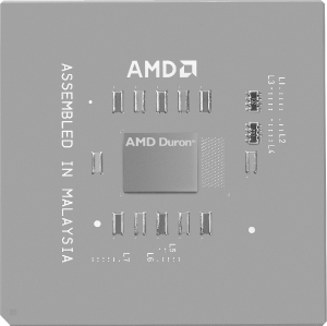
The Duron, code-named Spitfire and for a short time designated Athlon Value, was targeted at the value desktop market, and was to be a Celeron-killer. With it AMD straddled a fine line between matching Celeron clock speeds and performance on the one hand, versus avoiding cannibalizing sales of Athlon processors on the other. Accordingly, AMD differentiated the Duron by limiting the clock speed of the fastest current Duron to one step below the clock speed of the slowest current Athlon, by using a smaller and less efficient L2 cache, and by making the Duron only in 100 MHz FSB versions (versus the 133 MHz or higher FSB available on some Athlon models). The Spitfire-core Duron was an excellent processor for its time. It unquestionably offered more bang for the buck than any other processor sold by AMD or Intel. Although it achieved reasonable sales volumes in Europe, the Duron never really took off in the U.S. because of the absence of high-quality integrated Duron motherboards.
- Duron (Morgan core)
-
The Morgan-core Duron is simply a refresh of the Spitfire Duron to use the newer Palomino core. The advantages of the Morgan-core Duron over the Spitfire-core Duron are analogous to the advantages of the Palomino-core Athlon over the Thunderbird-core Athlon. The Morgan core is essentially a Palomino core with a smaller and less efficient L2 cache. As it did with the Spitfire, AMD carefully managed the Morgan to prevent cannibalizing sales of the Athlon XP. The fastest current Morgan was always at least one step slower than the slowest current Athlon XP. In terms of absolute performance clock for clock, the Morgan slightly outperforms the Coppermine-core Pentium III and the Tualatin-core Celeron.
The Appaloosa-core Duron, based on the Thoroughbred-core Athlon XP, was announced but later canceled. The Duron was a victim of AMD's success with the Athlon. As faster Athlons were introduced at lower prices, the Duron was simply squeezed out of its market niche. The Duron is still available as of July 2003, but is likely to disappear before year end. Figure 4-13 shows an AMD Duron processor.
Figure 4-13. AMD Duron processor (image courtesy of Advanced Micro Devices, Inc.)
- Athlon MP
-
Even the first Athlon processors had the circuitry needed to support dual-processor operation. That feature was useless until the introduction of the AMD-760MP chipset because no prior Athlon chipset supported dual processors. In mid-2001, Tyan shipped its 760MP-based Thunder motherboard. It supported dual Athlons, but was expensive and required a special power supply. In late 2001, Tyan shipped the inexpensive Tiger MP dual Athlon board, which used a standard power supply. Suddenly, dual Athlon systems were affordable, and many enthusiasts set out to build them.
AMD capitalized on this new market by introducing Athlon XP processors certified for dual-processor operation, which they named the Athlon MP. Athlon MP processors are binned (hand-picked and individually tested) for reliable SMP operation, or so the rumor has it. We have our doubts. We and many of our readers have run dual Athlon XPs successfully. Alas, AMD has disabled SMP operation on recent Athlon XP processors. If you want a dual Athlon system using current products, the only option is to use SMP-certified (and more expensive) Athlon MP processors. AMD has made Athlon MP processors using two cores:
- Athlon MP (Palomino core)
-
The first Athlon MP models used the Palomino core. They shipped in June 2001, four months before AMD introduced the first Palomino-core Athlon XP models. At that time, AMD had not yet decided to use model numbers rather than clock speeds to designate its processors, so the first two Athlon MP models were designated the Athlon MP/1.0G and the Athlon MP/1.2G. Those numbers accurately reflect their true clock speeds of 1000 MHz and 1200 MHz, respectively. By October 2001, when AMD began rolling out the new Palomino-core Athlon XPs, it had decided to designate the first model the Athlon XP/1500+, even though its actual clock speed was only 1333 MHz. All subsequent Athlon MP processors are designated by model number rather than clock speed. Functionally, the Palomino-core Athlon MP is identical to the Palomino-core Athlon XP.
- Athlon MP (Thoroughbred core)
-
Functionally, the Thoroughbred-core Athlon MP is identical to the Thoroughbred-core Athlon XP. When AMD transitioned to Thoroughbred-core Athlon XPs, it did not immediately introduce Athlon MP processors based on the Thoroughbred core. Instead, AMD began the staged introduction of Athlon MP processors that continues today. For example, in June 2002, AMD introduced Thoroughbred-core Athlon XP models 1700+ through 2200+. It was not until late August that AMD introduced Thoroughbred-core Athlon MP models at 2000+ and 2200+, just days after it introduced the Athlon XP 2400+ and 2600+. AMD says the delay is needed to certify faster models for SMP operation, which seems to us a reasonable explanation.
- Athlon MP (Barton core)
-
In May 2003 AMD shipped the Athlon MP 2800+, the first Athlon MP based on the Barton core. The 2800+ may also be the final Athlon MP model, because AMD now devotes all of its attention to the Opteron. Functionally, the Barton-core Athlon MP is identical to the Barton-core Athlon XP, including the increase from 256 KB to 512 KB of L2 cache. Interestingly, a few examples of the Athlon MP 2800+ with 333 MHz FSB have surfaced. We don't understand why AMD would produce such a processor. The 760MPX (the only Athlon chipset that supports SMP) supports a maximum FSB speed of 266 MHz, which seems to render a 333 MHz FSB Athlon MP pointless. We can only speculate that AMD plans a refresh of the 760MPX to add support for the 333 MHz FSB.
Table 4-5 lists the important characteristics of Socket A Duron and Athlon MP variants as of July 2003. For more information about these processors, see http://www.amd.com.
|
Duron |
Duron |
Athlon MP |
Athlon MP |
Athlon MP |
Athlon MP | |
|---|---|---|---|---|---|---|
|
Core |
Spitfire |
Morgan |
Palomino |
Palomino |
Thoroughbred |
Barton |
|
Model |
3 |
7 |
6 |
6 |
8 |
10 |
|
Production dates |
2000 - 2001 |
2001 - 2003 |
2001 - 2002 |
2001 - 2002 |
2002 - |
2003- |
|
Clock speeds (MHz) |
600, 650,700, 750,800, 850,900, 950 |
1000, 1100,1200, 1300 |
1000, 1200 |
1333, 1400,1533, 1600, 1667, 1733 |
1667, 1800, 2000, 2133 |
2133 |
|
Model designation |
n/a |
n/a |
n/a |
1500+, 1600+, 1800+, 1900+, 2000+, 2100+ |
2000+, 2200+, 2400+, 2600+ |
2800+ |
|
L2 cache size |
64 KB |
64 KB |
256 KB |
256 KB |
256 KB |
512 KB |
|
System bus speed |
200 MHz |
200 MHz |
266 MHz |
266 MHz |
266 MHz |
266 MHz |
|
Voltage (V) |
1.5V, 1.6V |
1.75V |
1.75V |
1.75V |
1.6V, 1.65V |
1.6V |
|
Dual CPU- capable |
-- |
-- |
|
|
|
|
|
Fabrication process |
0.18m |
0.18m |
0.18m |
0.18m |
0.13m |
0.13m |
|
Interconnects |
Cu |
Cu |
Cu |
Cu |
Cu |
Cu |
|
Die size (mm2) |
100 |
106 |
128 |
128 |
85 |
101 |
|
Transistors (million) |
25.00 |
25.18 |
37.2 |
37.2 |
37.5 |
54.3 |


