4.2 Intel Processors
Nearly all current PCs use either an Intel CPU or an Intel-compatible AMD Athlon CPU. The dominance of Intel in CPUs and Microsoft in operating systems gave rise to the hybrid term Wintel, which refers to systems that run Windows on an Intel or compatible CPU. Intel processors are referred to generically as x86 processors, based on Intel's early processor naming convention, 8086, 80186, 80286, etc. Intel has produced seven CPU generations, the first five of which are obsolete and the sixth obsolescent. They are as follows:
- First generation
-
The 8086 was Intel's first mainstream processor, and used 16 bits for both internal and external communications. The 8086 was first used in the late 1970s in dedicated word processors and minicomputers such as the DisplayWriter and the System/23 DataMaster. When IBM shipped its first PC in 1981, it used the 8088, an 8086 variant that used 16 bits internally but only 8 bits externally, because 8-bit peripherals were more readily available and less expensive then than were 16-bit components. The 8086 achieved prominence much later when Compaq created the DeskPro as an improved clone of the IBM PC/XT. A few early PCs, notably Radio Shack models, were also built around the 80186 and 80188 CPUs, which were enhanced versions of the 8086 and 8088 respectively. The 8088 and 8086 CPUs did not include an FPU, although an 8087 FPU, called a math coprocessor, was available as an optional upgrade chip. First generation Intel CPUs (or their modern equivalents) are still used in some embedded applications, but they are long obsolete as general-purpose CPUs.
- Second generation
-
In 1982, Intel introduced the long-awaited follow-on to its first generation processors. The 80286, based on the iAPX-32 core, provided a quantum leap in processor performance, executing instructions as much as five times faster than an 808x processor running at the same clock speed. The 80286 processed instructions as fast as many mainframe processors of the time. The 80286 also increased addressable memory from 1 MB to 16 MB, and introduced protected mode operations. The IBM PC/AT was the first commercial implementation of the 80286. The optional 80287 FPU chip added floating-point acceleration to 80286 systems. Although long obsolete as a general-purpose CPU, the 80286 is still used in embedded controllers.
- Third generation
-
Intel's next generation debuted in 1985 as the 80386, later shortened to just 386. The 386 was Intel's first 32-bit CPU, which communicated internally and externally with a 32-bit data bus and 32-bit address bus. The 386 was available in 16, 20, 25, and 33 MHz versions. Although 386 clock speeds were only slightly faster than those of the 80286, improved architecture resulted in significant performance increases. The optional 80387 FPU added floating-point acceleration to 386 systems. Intel later renamed the 386 to the 386DX and released a cheaper version called the 386SX, which used 32 bits internally but only 16 bits externally. The 386SX was notable as the first Intel processor that included an internal (L1) cache, although it was only 8 KB and relatively inefficient. The 386 is long obsolete as a general-purpose CPU, but it is still commonly used in embedded controllers.
- Fourth generation
-
Intel's next generation debuted in 1989 as the 486 (there never was an 80486). The 486 was a full 32-bit CPU with 8 KB of L1 cache, included a built-in FPU, and was available in speeds from 20 MHz to 50 MHz. Intel released 486DX and 486SX versions. The 486SX was in fact a 486DX with the FPU disabled. Intel also sold the 487SX, which was actually a full-blown 486DX. Installing a 487SX in the coprocessor socket simply disabled the existing 486SX. The 486DX/2, introduced in 1992, was the first Intel processor that ran internally at a multiple of the memory bus speed. The 486DX/2 clock ran at twice bus speed, and was available in 25/50, 33/66, and 40/80 MHz versions. The 486DX/4, introduced in 1994, ran (despite its name) at thrice bus speed, doubled L1 cache to 16 KB, and was available in 25/75, 33/100, and 40/120 versions. The 486 is obsolete as a general-purpose CPU, although it is still popular in embedded applications.
- Fifth generation
-
The Intel Pentium CPU defines the fifth generation. It provides much better performance than its 486 ancestors by incorporating several architectural improvements, most notably an increase in data bus width from 32 bits to 64 bits and an increase in CPU memory bus speed from 33 MHz to 60 and 66 MHz. Intel actually shipped several different versions of the Pentium, including:
Pentium P54?the original Pentium shipped in 1993 in 50, 60, and 66 MHz versions using a 1X CPU multiplier, ran (hot) at 5.0 volts, contained a dual 8 KB + 8 KB L1 cache, and fit Socket 4 motherboards.
Pentium P54C?the "Classic Pentium" first shipped in 1994, was available in speeds from 75 to 200 MHz using CPU multipliers from 1.5 to 3.0, used 3.3 volts, and contained the same dual L1 cache as the P54. P54C CPUs fit Socket 5 motherboards and most Socket 7 motherboards.
Pentium P55C?the Pentium/MMX shipped in 1997, was available in speeds from 166 to 233 MHz, using CPU multipliers from 2.5 to 3.5, used 3.3 volts, and contained a dual 16 KB + 16 KB L1 cache, twice the size of earlier Pentiums. The other major change from the P54C was the addition of the MMX instruction set, a set of additional instructions that greatly improved graphics processing speed. P55C CPUs fit Socket 7 motherboards, and are still in limited distribution as of July 2003.
The Pentium and other fifth-generation processors are obsolete, although millions of Pentium systems remain in service. Any system that uses a fifth-generation processor is too old to upgrade economically.
- Sixth generation
-
This generation began with the 1995 introduction of the Pentium Pro, and includes the Pentium II, Celeron, and Pentium III processors. Late sixth-generation Intel desktop processors had been relegated to entry-level systems by early 2002 and had been discontinued as mainstream products by mid-2002. By late 2002, only the Tualatin-core Celeron processors remained as representatives of this generation. Although it is still technically feasible to upgrade the processor in many sixth-generation systems, in practical terms it usually makes more sense to replace the motherboard and processor with seventh-generation products.
- Seventh generation
-
This is the current generation of Intel processors, and includes Intel's flagship Pentium 4 as well as various Celeron processors based on the Pentium 4 architecture.
Intel currently manufactures several sixth-generation processors, including numerous variants and derivatives of the Celeron and Pentium III, and two seventh-generation processors, the Pentium 4 and the Celeron. The following sections describe current and recent Intel processors.
|
4.2.1 Pentium, Pentium/MMX
Intel originally designated its processors by number rather than by name?Intel 8086, 8088, 80186, 80286, and so on. Intel dropped the "80" prefix early in the life cycle of the 80386, relabeling it as the 386. (Intel never made an "80486" processor despite what some people believe.) By the time Intel shipped its fourth-generation processors, it was tired of other makers using similar names for their compatible processors. Intel believed that these similar names could lead to confusion among customers, and so tried to trademark its X86 naming scheme. When Intel learned that part numbers cannot be trademarked, the company decided to drop the "86" naming scheme and create a made-up word to name its fifth generation processors. Intel came up with Pentium.
Intel has produced the following three major subgenerations of Pentium:
- P54
-
These earliest Pentium CPUs, first shipped in March 1993, fit Socket 4 motherboards, use a 3.1 million transistor core, have 16 KB L1 cache, and use 5.0 volts for both core and I/O components. P54-based systems use a 50, 60, or 66 MHz memory bus and a fixed 1.0 CPU multiplier to yield processor speeds of 50, 60, or 66 MHz.
- P54C
-
The so-called Classic Pentium CPUs, first shipped in October 1994, fit Socket 5 and most Socket 7 motherboards, use a 3.3 million transistor core, have 16 KB L1 cache, and generally use 3.3 volts for both core and I/O components. P54C-based systems use a 50, 60, or 66 MHz memory bus and CPU multipliers of 1.5, 2.0, 2.5, and 3.0x to yield processor speeds of 75, 90, 100, 120, 133, 150, 166, and 200 MHz.
- P55C
-
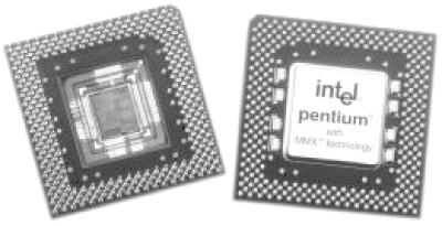
The Pentium/MMX CPUs (shown in Figure 4-1), first shipped in January 1997, fit Socket 7 motherboards, use a 4.1 million transistor core, have a 32 KB L1 cache, feature improved branch prediction logic, and generally use a 2.8 volt core and 3.3 volt I/O components. P55C-based systems use a 60 or 66 MHz memory bus and CPU multipliers of 2.5, 3.0, 3.5, 4.0, 4.5, and 5.0x to yield processor speeds of 120, 133, 150, 166, 200, 233, 266, and 300 MHz.
Figure 4-1. Intel Pentium/MMX processor (photo courtesy of Intel Corporation)
The Pentium was a quantum leap from the 486 in complexity and architectural efficiency. It is a CISC processor, and was initially built on a 0.35 micron process (later 0.25 micron). Pentiums, like 486s, use 32-bit operations internally. Externally, however, the Pentium doubles the 32-bit 486 data bus to 64 bits, allowing it to access eight full bytes at a time from memory. With the Pentium, Intel also introduced new chipsets to support this wider data bus and other Pentium enhancements.
The Pentium uses a dual-pipelined superscalar design which, relative to the 486 and earlier CPUs, allows it to execute more instructions per clock cycle. The Pentium executes integer instructions using the same five stages as the 486?Prefetch, Instruction Decode, Address Generate, Execute, and Write Back?but the Pentium has two parallel integer pipelines versus the 486's one, which allows the Pentium to execute two integer operations simultaneously in parallel. This means that, for equal clock speeds, the Pentium processes integer instructions about twice as fast as a 486.
The Pentium includes an improved 80-bit FPU that is much more efficient than the 486 FPU. The Pentium also includes a Branch Target Buffer to provide dynamic branch prediction, a process that greatly enhances instruction execution efficiency. Finally, the Pentium includes a System Management Module that can control power use by the processor and peripherals.
P54 Pentiums also improved upon 486 L1 caching. The 486 has one 8 KB L1 cache (16 KB for the 486DX/4) that uses the inefficient write-through algorithm. P54 and P54C Pentiums have dual 8 KB L1 caches?one for data and one for instructions?that use the much more efficient two-way set associative write-back algorithm. This doubling of L1 cache buffers and the improved caching algorithm combined to greatly enhance CPU performance. P55C Pentiums double L1 cache size to 16 KB, providing still more improvement.
The changes from the P54 to the P54C were relatively minor. Higher voltages and faster CPU speeds generate more heat, so Intel reduced the core and I/O voltages from 5.0/5.0V in the P54 to 3.3/3.3V in the P54C, allowing them to run the CPUs faster without excessive heating. Intel also introduced support for CPU multipliers, which allow the CPU to run internally at some multiple of the memory bus speed.
The changes from the P54C Classic to the P55C MMX were much more significant. In fact, had Intel not already introduced the Pentium Pro (its first sixth-generation CPU) before the P55C, the P55C might have been considered the first of a new CPU generation. In addition to doubling L1 cache size, the P55C incorporated two major architectural enhancements:
- MMX
-
Although sometimes described as MultiMedia eXtensions or Matrix Math eXtensions, Intel says officially that MMX stands for nothing. MMX is a set of 57 added instructions that are dedicated to manipulating audio, video, and graphics data more efficiently.
- SIMD
-
Single Instruction Multiple Data (SIMD) is an architectural enhancement that allows one instruction to operate simultaneously on multiple sets of similar data.
In conjunction, MMX and SIMD greatly extend the Pentium's ability to perform parallel operations, processing 8 bytes of data per clock cycle rather than 1 byte. This is particularly important for heavily graphics-oriented operations such as video because it allows the P55C to retrieve and process eight 1-byte pixels in one operation rather than manipulating those 8 bytes as 8 separate operations. Intel estimates that MMX and SIMD used with nonoptimized software yield performance increases of as much as 20%, and can yield increases of 60% when used with MMX-aware applications.
Although the Pentium is technically obsolete, millions of Pentium systems remain in service as Linux firewalls or as dedicated appliance servers, and a significant number of them continue to be upgraded. As of July 2003 Intel still produced the Pentium/200 and /233 MMX processors in Socket 7, as well as several slower models for embedded applications. For additional information about Pentium processors, including detailed identification tables, visit http://developer.intel.com/design/pentium/.
4.2.2 Pentium Pro
Intel's first sixth-generation CPU, the Pentium Pro, was introduced in November 1995?along with the new 3.3 volt 387-pin Socket 8 motherboards required to accept it?and was discontinued in late 1998. Pentium Pro processors are no longer made, but remain available on the used market. Intel positioned the Pentium Pro for servers, a niche it never escaped, and where it continued to sell in shrinking numbers until its replacement, the Pentium II Xeon, shipped in mid-1998. The Pentium Pro predated the P55C Pentium/MMX, and never shipped in an MMX version. The Pentium Pro never sold in large numbers for two reasons:
- Cost
-
The Pentium Pro was a very expensive processor to build. Its core logic comprised 5.5 million transistors (versus 4.1 million in the P55C), but the real problem was that the Pentium Pro also included a large L2 cache on the same substrate as the CPU. This L2 cache required millions of additional transistors, which in turn required a much larger die size and resulted in a much lower percentage yield of usable processors, both factors that kept Pentium Pro prices very high relative to other Intel CPUs.
- 32-bit optimization
-
The Pentium Pro was optimized to execute 32-bit operations efficiently at the expense of 16-bit performance. For servers, 32-bit optimization is ideal, but slow 16-bit operations meant that a Pentium Pro actually ran many Windows 95 client applications slower than a Pentium running at the same clock speed.
The Pentium Pro shipped in 133, 150, 166, 180, and 200 MHz versions with 256 KB, 512 KB, or 1 MB of L2 cache, and was never upgraded to a faster version. The Pentium Pro continued to sell long after the introduction of much faster Pentium II CPUs for only one reason: the first Pentium II chipsets supported only two-way Symmetric Multiprocessing (SMP) while Pentium Pro chipsets supported four-way SMP. In some server environments, four 200 MHz Pentium Pro CPUs outperformed two 450 MHz Pentium II CPUs. The introduction of the 450NX chipset, which supports four-way SMP, and the mid-1998 introduction of the Pentium II Xeon processor, which supports eight-way SMP, removed the raison d'être for the Pentium Pro, and it died a quick death.
4.2.2.1 Pentium Pro processor architecture
Although the Pentium Pro is obsolete, it was the first Intel sixth-generation processor, and as such introduced many important architectural improvements. Understanding the Pentium Pro vis-à-vis the Pentium will help you understand current Intel CPU models. The two CPUs differ in the following major respects:
- Secondary (L2) cache
-
Pentium-based systems may optionally be equipped with an external L2 secondary cache of any size supported by the chipset. Typical Pentium systems have a 256 KB L2 cache, but high-performance motherboards may include a 512 KB, 1 MB, or larger L2 cache. But Pentium L2 caches use a narrow (32-bit), slow (60 or 66 MHz memory bus speed) link between the processor's L1 cache and the L2 cache. The Pentium Pro L2 cache is internal, located on the CPU itself, and the Pentium Pro uses a 64-bit data path running at full processor speed to link L1 cache to L2 cache. The dedicated high-speed bus used to connect to cache is called the Backside Bus (BSB), as opposed to the traditional CPU-to-chipset bus, which is now designated the Frontside Bus (FSB). In conjunction, the BSB and FSB are called the Dual Independent Bus (DIB) architecture. DIB architecture yields dramatically improved cache performance. In effect, 256 KB of Pentium Pro L2 cache provides about the same performance boost as 2 MB or more of Pentium L2 cache.
- Dynamic execution
-
The Pentium Pro uses a combination of techniques?including branch prediction, data flow analysis, and speculative execution?that collectively are referred to as dynamic execution. Using these techniques, the Pentium Pro productively uses clock cycles that would otherwise be wasted, as they are with the Pentium.
- Super-pipelining
-
Super-pipelining is a technique that allows the Pentium Pro to use out-of-order instruction execution, another method to avoid wasting clock cycles. The Pentium executes instructions on a first-come, first-served basis, which means that it waits for all required data to process an earlier instruction instead of processing a later instruction for which it already has all of the data. Because it uses linear instruction sequencing, or standard pipelining, the Pentium wastes what could otherwise be productive clock cycles executing no-op instructions. The Pentium Pro is the first Intel CPU to use super-pipelining. It has a 14-stage pipeline, divided into three sections. The first section, the in-order front end, comprises eight stages, and decodes and issues instructions. The second section, the out-of-order core, comprises three stages, and executes instructions in the most efficient order possible based on available data, regardless of the order in which it received the instructions. The third and final section, the in-order retirement section, receives and forwards the results of the second section.
- CISC versus RISC core
-
The most significant architectural difference between the Pentium and the sixth-generation processors is how they handle instructions internally. Pentiums use a Complex Instruction Set Computer (CISC) core. CISC means that the processor understands a large number of complicated instructions, each of which accomplishes a common task in just one instruction. The Pentium Pro was the first Intel CPU to use a Reduced Instruction Set Computer (RISC) core. RISC means that the processor understands only a few simple instructions. Complex operations are performed by stringing together multiple simple instructions. Although RISC CPUs must perform many simple instructions to accomplish the same task that CISC CPUs do with just one or a few complex instructions, the simple RISC instructions execute much faster than CISC instructions.
The Pentium Pro translates standard Intel x86 CISC instructions into RISC instructions that the Pentium Pro microcode uses internally, and then passes those RISC instructions to the internal out-of-order execution core. This translation helps avoid limitations of the standard x86 CISC instruction set, and supports the out-of-order execution that prevents pipeline stalls, but those benefits come at a price. Although the time required is measured in nanoseconds, converting from CISC to RISC does take time, and that slows program execution. Also, 16-bit instructions convert inefficiently and frequently result in pipeline stalls in the out-of-order execution unit, which commonly result in CPU wait states of as many as seven clock cycles. The upshot is that, for pure 32-bit operations, the benefit of RISC conversion greatly outweighs the drawbacks, but for 16-bit operations, the converse is true.
For additional information about Pentium Pro processors, including detailed identification tables, visit http://developer.intel.com/design/pro/.
4.2.3 Pentium II Family
Intel's first mainstream sixth-generation CPU, the Pentium II, shipped in May 1997. Intel subsequently shipped many variants of the Pentium II, which differ chiefly in packaging, the type and amount of L2 cache they include, the processor core they use, and the FSB speeds they support. All members of the Pentium II family use the Dynamic Execution Technology and DIB architecture introduced with the Pentium Pro. Intel reduced the core voltage from the 3.3 volts used by Pentium Pro to 2.8 volts or less in Pentium II processors, which allows them to run much faster while using less power and producing less heat. In effect, you're not far wrong if you think of Pentium II, sixth-generation Celeron, and Pentium III processors as faster versions of the Pentium Pro with MMX (or the enhanced SSE version of MMX) added, and the following major changes:
- L2 cache
-
The Pentium Pro taught Intel the folly of embedding the L2 cache onto the CPU substrate itself, at least for the then-current state of the technology. Early Pentium II family processors use discrete L2 cache Static RAM (SRAM) chips that reside within the CPU package but are not a part of the CPU substrate. Advances in fab technology have allowed Intel again to place L2 cache directly on the processor substrate on later Pentium II family processor models. Some Pentium II family processors run L2 cache at full processor speed, while others run it at half processor speed. The least-expensive Pentium II family processors have no L2 cache at all. The L2 cache in later members of the Pentium II family is improved, not just in size and/or speed, but also in functionality. The most recent Pentium III processors, for example, use an eight-way set associative cache, which is more efficient than the caching schemes used on earlier variants.
- Packaging
-
The Pentium Pro used the huge, complicated 387-pin Dual Pattern-Staggered Pin Grid Array (DP-SPGA) Socket 8. The extra pins provide data and power lines for the onboard L2 cache. Intel developed simplified alternative packaging methods for various members of the Pentium II family processors, which are described later in this chapter.
- Improved 16-bit performance
-
High cost aside, the major reason the Pentium Pro was never widely used other than in servers was its poor performance with 16-bit software. Although represented as a 32-bit operating system, Windows 95/98 still contains much 16-bit code. Users quickly discovered that Windows 95 actually ran slower on a Pentium Pro than on a Pentium of the same speed. Intel solved the 16-bit problem by using the Pentium segment descriptor cache in the Pentium II.
Members of the Pentium II family include the Pentium II, Pentium II Overdrive, Pentium II Xeon, sixth-generation Celeron, Pentium III, and Pentium III Xeon. Each of these processors is described in the following sections.
4.2.3.1 Pentium II
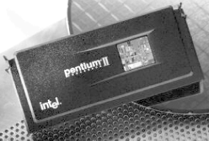
First-generation Pentium II processors shipped in 233, 266, 300, and 333 MHz versions with the Klamath core and a 66 MHz FSB. In mid-1998, Intel shipped second-generation Pentium II processors, based on the Deschutes core, that ran at 350, 400, and 450 MHz and used a 100 MHz FSB. Pentium II processors have 512 KB of L2 cache that runs at half internal CPU speed versus 256 KB to 1 MB of full CPU speed L2 cache in the Pentium Pro. Pentium II processors use a Single Edge Contact connector (SECC) or SECC2 cartridge, which contains the CPU and L2 cache (see Figure 4-2). The SECC/SECC2 package mates with a 242-contact slot connector, formerly known as Slot 1, which resembles a standard expansion slot. Klamath-based processors run at 2.8 volts and are built on a 0.35m fab. Deschutes-based processors, including all 100 MHz FSB processors and recent 66 MHz FSB processors, run at 2.0 volts and are built on a 0.25m fab. Excepting FSB speed and fab process, all Slot 1 Pentium II processors are functionally identical. As of July 2003, Pentium II processors remain in limited distribution, but they are obsolescent.
Figure 4-2. Intel Pentium II processor in the original SECC package (photo courtesy of Intel Corporation)
For additional information about Pentium II processors, including detailed identification tables, visit http://developer.intel.com/design/pentiumii/. For information about the Pentium II Xeon processor, see http://www.intel.com/support/processors/pentiumii/xeon/.
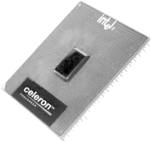
4.2.3.2 Celeron
The sixth-generation Celeron?we keep saying "sixth-generation" because Intel also makes a seventh-generation Celeron based on the Pentium 4?was initially an inexpensive variant of the Pentium II and, in later models, an inexpensive variant of the Pentium III. Klamath-based (Covington-core) Celerons shipped in April 1998 in 266 and 300 MHz versions without L2 cache. Performance was poor, so in fall 1998 Intel began shipping modified Deschutes-based (Mendocino- core) Celerons with 128 KB L2 cache. The smaller Celeron L2 cache runs at full CPU speed, and provides L2 cache performance similar to that of the larger but slower Pentium II L2 cache for most applications. Mendocino (0.25m) Celerons have been manufactured in 300A (to differentiate it from the cacheless 300), 333, 366, 400, 433, 466, 500, and 533 MHz versions, all of which use the 66 MHz FSB.
With the introduction of the Coppermine-core Pentium III processor, Intel also introduced Celeron processors based on a variant of the Coppermine core called the Coppermine128 core. Celerons based on this 0.18m, 1.6v core began shipping in 533A, 566, and 600 MHz versions soon after their announcement in May 2000, and were eventually produced in speeds as high as 1.1 GHz, which approaches the limit of the Coppermine core itself.
Coppermine128-core Celerons have half of the 256 KB on-die L2 cache disabled to bring L2 cache size to the Celeron-standard 128 KB, and use a four-way set associate L2 cache rather than the eight-way version used by the Coppermine Pentium III. Coppermine128-core Celerons through the Celeron/766, shipped in November 2000, use the 66 MHz FSB speed. Coppermine128-core Celerons that use the 100 MHz FSB speed began shipping in March 2001, beginning with 800 MHz units and eventually reaching 1.1 GHz. Other than the differences in L2 cache size and type, processor bus speed differences, and official support for SMP, Coppermine128-core Celerons support the standard Coppermine-core Pentium III features, including SSE, described later in this chapter.
|
In November 2001, Intel began shipping Celerons based on the latest Pentium III core, code-named Tualatin. The first Tualatin-core Celerons ran at 1.2 GHz using the 100 MHz FSB. Intel later filled in the product line by shipping 100 MHz FSB Tualatin-core Celerons at 900 MHz, 1.0 GHz, 1.1 GHz, 1.3 GHz, and finally 1.4 GHz. Tualatin-core Celerons also differ from earlier Celeron models in that they include a full 256 KB eight-way set associative L2 cache, the same as Coppermine-core Pentium III models. Tualatin-core Celerons perform like full-blown Pentium IIIs because they effectively are full-blown Pentium IIIs.
So why did Intel suddenly decide to uncripple the Celeron? Basically, it had devoted a lot of resources to developing the Tualatin-core Pentium III only to find itself overtaken by events. Intel needed to ship the Pentium 4 to counter fast AMD Athlons, but there was no room in Intel's lineup for two premium processors. Accordingly, the Pentium III had to go, at least as mainstream product, giving way to the new-generation Pentium 4. But that left Intel with the perfectly good, new Tualatin core, which had been developed at great expense, with no way to sell it. Talk about being all dressed up with nowhere to go.
As a way of earning back the development costs of the Tualatin core while at the same time putting the screws to AMD's low-end Duron, Intel decided to ship Pentium III processors with the Celeron name on them. The new Celerons handily outperformed Durons running at the same clock speed, and in fact were surprisingly close to the performance level of the fastest Pentium 4 and Athlon processors then available. Selling for less than $100, the Tualatin-core Celerons provided incredibly high bang for the buck. In fact, they still do today. A Celeron/1.4G running in an 815-based motherboard is slower than a fast Pentium 4 and Athlon system, certainly, but is by no means a slow system.
Celerons have been produced in four form factors:
- Single Edge Processor Package cartridge
-
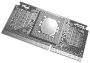
All Celerons through 433 MHz were produced in Single Edge Processor Package (SEPP) cartridge form, which resembles the Pentium II SECC and SECC2 package, and is compatible with the Pentium II 242-contact slot. In mid-1999 Intel largely abandoned SEPP in favor of PPGA, and SEPP Celerons are no longer available new. Figure 4-3 shows an SEPP Celeron.
Figure 4-3. Intel Celeron processor in SEPP package (photo courtesy of Intel Corporation)
- Plastic Pin Grid Array
-
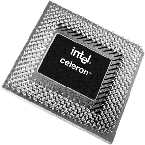
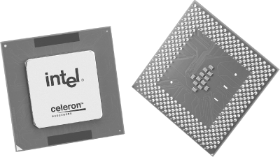
As a cheaper alternative to SEPP, Intel developed the Plastic Pin Grid Array (PPGA). PPGA processors fit Socket 370, which resembles Socket 7 but accepts only PPGA Celeron and Pentium III processors. All Mendocino-core Celerons are manufactured in PPGA. The Celeron/466 was the first Celeron produced only in PPGA. PPGA processors can be used in most Socket 370 motherboards, although a few accept only Socket 370 Pentium III processors. PPGA Celerons are no longer available new. Figure 4-4 shows a PPGA Celeron.
Figure 4-4. Intel Celeron processor in PPGA package (photo courtesy of Intel Corporation)
- Flip Chip Pin Grid Array
-
With the introduction of the Socket 370 version of the Pentium III, Intel introduced a modified version of PPGA called Flip Chip PGA (FC-PGA), which uses slightly different pinouts than PPGA. FC-PGA essentially reverses the position of the processor core from PPGA, placing the core on top (where it can make better contact with the heatsink) rather than on the bottom side with the pins. All Socket 370 Pentium III and Coppermine128-core Celerons (the 533A, 566, 600, and faster versions) require an FC-PGA compliant motherboard. FC-PGA processors physically fit older PPGA motherboards, but if you install an FC-PGA processor in a PPGA-only Socket 370 motherboard the processor doesn't work, although no harm is done. FC-PGA Celerons are no longer available new. Figure 4-5 shows an FC-PGA Celeron.
Figure 4-5. Intel Celeron processor in FC-PGA package (photo courtesy of Intel Corporation)
- Flip Chip Pin Grid Array 2
-
Tualatin-core Celerons use the FC-PGA2 packaging, which is essentially FC-PGA with the addition of a flat metal plate, called an Integrated Heat Spreader, that covers the processor chip itself. Although these processors physically fit any Socket 370 motherboard, only very recent Socket 370 chipsets support the Tualatin core. Intel designates its own motherboard models that support Tualatin as "Universal" models. Other manufacturers use other terminology, but the important thing to remember is that the motherboard must explicitly support Tualatin if it is to run these processors. As of July 2003, Intel still produces FC-PGA Celerons in 1.0, 1.1, 1.2, 1.3, and 1.4 GHz models. Figure 4-6 shows an FC-PGA2 Celeron.
Figure 4-6. Intel Celeron processor in FC-PGA2 package (photo courtesy of Intel Corporation)
Intel has produced five major variants of the Celeron, using four packages, four cores, two bus speeds, four fab sizes, and more than 20 clock speeds. Table 4-1 summarizes the major differences between these variants.
|
Covington |
Mendocino |
Coppermine128 |
Coppermine128 |
Tualatin | |
|---|---|---|---|---|---|
|
Package |
SECC |
SECC-2PPGA |
FC-PGA |
FC-PGA |
FC-PGA2 |
|
Manufacturing dates |
1998 |
1998 - 2000 |
2000 - 2002 |
2001 - 2002 |
2001 - |
|
Clock speeds (MHz) |
266, 300 |
300A, 333, 366, 400, 433, 466, 500, 533 |
500A, 533A, 566, 600, 633, 667, 700, 733, 766 |
800, 850, 900, 950, 1000, 1100 |
900, 1000, 1100, 1200, 1300, 1400 |
|
L2 cache size |
none |
128 KB |
128 KB |
128 KB |
256 KB |
|
L2 cache bus width |
n/a |
64 bits |
256 bits |
256 bits |
256 bits |
|
System bus speed |
66 MHz |
66 MHz |
66 MHz |
100 MHz |
100 MHz |
|
SSE instructions |
-- |
-- |
|
|
|
|
Dual CPU capable |
|
|
-- |
-- |
-- |
|
Fabrication process |
0.35m |
0.25m |
0.18m |
0.18m |
0.13m |
Dual-CPU capability deserves an explanation. Although Intel never officially supported Celerons for SMP operation, the two earliest Celeron variants did in fact support dual-CPU operation. For Covington-core and SECC-2 Mendocino-core Celerons, dual-CPU operation was impractical because enabling SMP required physical surgery on the processor package?literally drilling holes in the package and soldering wires. With PPGA Mendocino-core Celerons, dual-CPU operation was eminently practical because many dual Socket 370 motherboards were designed specifically to accept two Celerons, and no changes to the processors themselves were necessary. Beginning with the 66 MHz Coppermine128 Celerons, Intel physically disabled SMP operation in the core itself, so it is impossible to operate Coppermine- or Tualatin-core Celerons in SMP mode.
For additional information about Celeron processors, including detailed identification tables, visit http://developer.intel.com/design/celeron/.
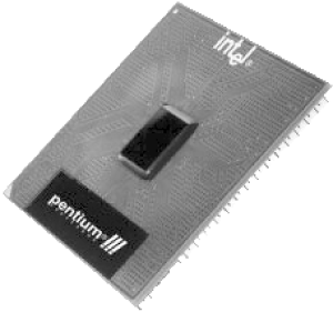
4.2.3.3 Pentium III
The Pentium III, Intel's final sixth-generation processor, began shipping in February 1999. The Pentium III has been manufactured in numerous variants, including speeds from 450 MHz to 1.4 GHz (Intel defines 1 GHz as 1000 MHz), two bus speeds (100 MHz and 133 MHz), four packages (SECC, SECC2, FC-PGA, and FC-PGA2), and the following three cores:
- Pentium III (Katmai core)
-
Initial Pentium III variants use the Katmai core, essentially an enhanced Deschutes with the addition of 70 new Streaming SIMD instructions (formerly called Katmai New Instructions or KNI and known colloquially as MMX/2) that improve 3D graphics rendering and speech processing. They use the 0.25m process, operate at 2.0V core voltage (with some versions requiring marginally higher voltage), use a 100 or 133 MHz FSB, incorporate 512 KB four-way set associative L2 cache running at half CPU speed, and have glueless support for two-way SMP. Katmai-core processors were made in SECC2 (Slot 1/SC242) at 450, 500, 550, and 600 MHz in 100 MHz FSB variants, and at 533 and 600 MHz in 133 MHz FSB variants.
- Pentium III (Coppermine core)
-
Later Pentium III variants use the Coppermine core, which is essentially a refined version of the Katmai core. Later Coppermine processors use the updated Coppermine-T core. Coppermine processors use the 0.18m process, which reduces die size, heat production, and cost. They operate at nominal 1.6V core voltage (with faster versions requiring marginally higher voltage), are available at either 100 MHz or 133 MHz FSB, and (in most variants) support SMP. Coppermine-core processors have been made in SECC2 (Slot 1/SC242) and FC-PGA (Socket 370) packaging in both 100 and 133 MHz FSB variants, running at speeds from 533 MHz to 1.13 GHz. Finally, Coppermine also incorporates the following significant improvements in L2 cache implementation and buffering:
- Advanced Transfer Cache
-
Advanced Transfer Cache (ATC) is how Intel summarizes the several important improvements in L2 cache implementation from Katmai to Coppermine. Although L2 cache size is reduced from 512 KB to 256 KB, it is now on-die (rather than discrete SRAM chips) and, like the Celeron, operates at full CPU speed rather than half. Bandwidth is also quadrupled, from the 64-bit bus used on Katmai- and Mendocino-core Celeron processors to a 256-bit bus. Finally, Coppermine uses an eight-way set associative cache, rather than the four-way set associative cache used by earlier Pentium III and Celeron processors. Migrating L2 cache on-die increased transistor count from just under 10 million for the Katmai to nearly 30 million for Coppermine, which may account for the reported early yield problems with the Coppermine.

When manufacturers begin producing a processor, a relatively high percentage of the processors made are unusable. In the initial phases, many of the processors on each wafer may be spoiled. As the manufacturer ramps up production and gains experience, the percentage of usable processors increases substantially, as does the percentage of processors that are usable at higher speeds. Marketing reasons aside, yield percentage is the major factor in the very high price of the fastest processors. During early production, only 1% to 10% of the processors produced may be able to run at the highest speed offered for that processor. As the yield percentage improves, manufacturers can cut processor prices. Yield percentages are one of the most closely guarded secrets in semiconductor manufacturing.
- Advanced System Buffering
-
Advanced System Buffering (ASB) is how Intel describes the increase from Pentium III Katmai and earlier processors to the Coppermine from four to six fill buffers, four to eight queue entry buffers, and one to four writeback buffers. The increased number of buffers was primarily intended to prevent bottlenecks with 133 MHz FSB Coppermines, but also benefits those running at 100 MHz.
- Pentium III (Tualatin core)
-
The latest Pentium III variants use the Tualatin core, which is the last Pentium III core Intel will ever produce. Tualatin processors use the 0.13m process, which reduces die size, heat production, and cost, and allows considerably higher clock speeds than the Coppermine core. Had it not been for Intel's rapid transition to the Pentium 4, Tualatin-core Pentium IIIs could have been Intel's flagship processor through at least the end of 2002. Intel could have shipped Tualatins at ever-increasing clock speeds, beating the 0.18m Palomino-core AMD Athlon on both clock speed and actual performance. Instead, Intel opted to compete using the Pentium 4. Intel has by its pricing mechanism effectively exiled Tualatin-core Pentium IIIs to niche status by selling fast Pentium 4 processors for less than Tualatin Pentium IIIs with comparable performance.
Tualatins use the 133 MHz FSB, and are available in two major variants, both of which use the FC-PGA2 packaging (with Integrated Heat Spreader). The first variant, intended for desktop systems, has the standard 256 KB L2 cache, uses the 133 MHz FSB, and was made in 1.0, 1.13, 1.2, 1.33, and 1.4 GHz models. The second variant, intended for entry-level servers and workstations, has 512 KB L2 cache, uses the 100 or 133 MHz FSB, and was made in models that run at 700, 800, 900, or 933 MHz, as well as models that run at 1.13, 1.26, and 1.4 GHz. Both variants are SMP-capable. Finally, Intel removed the much-hated Processor Serial Number from all Tualatin-core processors.
Table 4-2 summarizes the important differences between Pentium III variants as of July 2003. When necessary to differentiate processors of the same speed, Intel uses the E suffix to indicate support for ATC and ASB, the B suffix to indicate 133 MHz FSB, and the EB suffix to indicate both. An A suffix designates 0.13m Tualatin-core processors. All processors faster than 600 MHz include both ATC and ASB. Note that A-step FC-PGA processors do not support SMP. B-step and higher FC-PGA and FC-PGA2 processors support SMP, except the 1B GHz processor, which is not SMP-capable in any stepping.
|
1.40, 1.26,1.13 GHz |
1.33, 1.20,1.13A,1A GHz |
1B GHz,933, 866, 800EB, 733, 667, 600EB, 533EB |
850, 800, 750, 700, 650, 600E, 550E |
1.10G, 1G, 850, 800, 750, 700, 650, 600, 550E, 500E |
1G, 933, 866, 800, 733, 667, 600EB, 533EB |
600B, 533B |
600, 550, 500, 450 | |
|---|---|---|---|---|---|---|---|---|
|
Package |
FC-PGA2 |
FC-PGA2 |
SECC2 |
SECC2 |
FC-PGA |
FC-PGA |
SECC2 |
SECC2 |
|
Process size |
0.13m |
0.13m |
0.18m |
0.18m |
0.18m |
0.18m |
0.25m |
0.25m |
|
FSB speed (MHz) |
133 |
133 |
133 |
100 |
100 |
133 |
133 |
100 |
|
L2 cache size (KB) |
512 |
256 |
256 |
256 |
256 |
256 |
512 |
512 |
|
L2 cache speed |
CPU |
CPU |
CPU |
CPU |
CPU |
CPU |
1/2 CPU |
1/2 CPU |
|
SMP support |
|
|
|
|
|
|
|
|
|
Process or S/N |
-- |
-- |
|
|
|
|
|
|
|
Figure 4-7 shows a Pentium III processor in the SECC2 package. Some early Pentium III models were produced in the original SECC package, which closely resembles the Pentium II SECC package shown in Figure 4-2. Figure 4-8 shows a Pentium III processor in the FC-PGA package. Other than labeling, the Pentium III processor in the FC-PGA2 package closely resembles the FC-PGA2 Celeron processor shown in Figure 4-6.
Figure 4-7. Intel Pentium III processor in SECC2 package (photo courtesy of Intel Corporation)
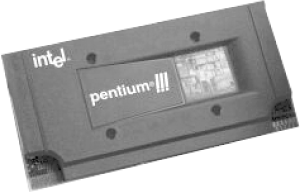
Figure 4-8. Intel Pentium III processor in FC-PGA package (photo courtesy of Intel Corporation)
For additional information about Pentium III processors, including detailed identification tables, visit http://developer.intel.com/design/pentiumiii/. For information about Pentium III Xeon processors, visit http://developer.intel.com/design/pentiumiii/xeon/.
4.2.4 Pentium 4
By late 2000, Intel found itself in a conundrum. In March of that year, AMD had forced Intel's hand by releasing an Athlon running at 1 GHz. Intel planned to release a 1.0 GHz version of its flagship processor, the Coppermine-core Pentium III, but not until much later. The Athlon/1.0G introduction was a wakeup call for Intel. It had to ship a Pentium III/1.0G immediately if it was to remain competitive on clock speed with the Athlon. One week after the Athlon/1.0G shipped, Intel shipped a Pentium III running at the magic 1.0 GHz.
The problem was that the Pentium III Coppermine core effectively topped out at about 1.0 GHz, while the Athlon Thunderbird core had plenty of headroom. For the next several months, AMD shipped faster and faster Athlons, while Intel remained stuck at 1.0 GHz. And to make matters worse, AMD could ship fast Athlons in volume, while Intel had very low yields on the fast Pentium III parts. Although 1.0 GHz Pentium IIIs were theoretically available, in reality even the 933 MHz parts were hard to come by. So Intel had to make the best of things, shipping mostly sub-900 MHz Pentium IIIs while AMD claimed the high end. Intel must have been gritting its collective teeth.
Adding insult to injury, Intel attempted unsuccessfully to ship a faster Pentium III, the ill-fated Pentium III/1.13G. These processors were available in such small volumes that many observers believed they must be almost handmade. Adding to Intel's embarrassment, popular enthusiast web sites including Tom's Hardware (http://www.tomshardware.com) and AnandTech (http://www.anandtech.com) reported that the 1.13 GHz parts did not function reliably. Intel was forced to admit this was true and withdrew the 1.13 GHz part, although it later reintroduced it successfully.
Intel had two possible responses to the growing clock speed gap. It could expedite the release of 0.13m Tualatin-core Pentium IIIs, which have clock speed headroom at least equivalent to the Thunderbird-core and later Palomino-core Athlons, or it could introduce its seventh-generation Pentium 4 processor sooner than planned (see Figure 4-9). Intel wasn't anywhere near ready to convert its fabs to 0.13m Tualatin-core Pentium III production, so its only real choice was to get the Pentium 4 to market quickly.
There were several problems with that course, not the least of which were that the 0.18m Willamette-core Pentium 4 was not really ready for release and the


